


Mikroelektronika d.o.o.
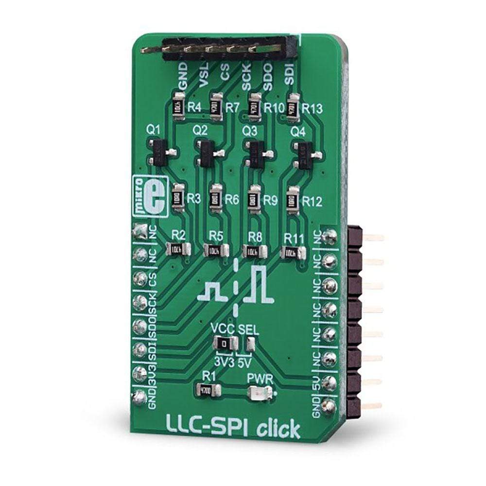
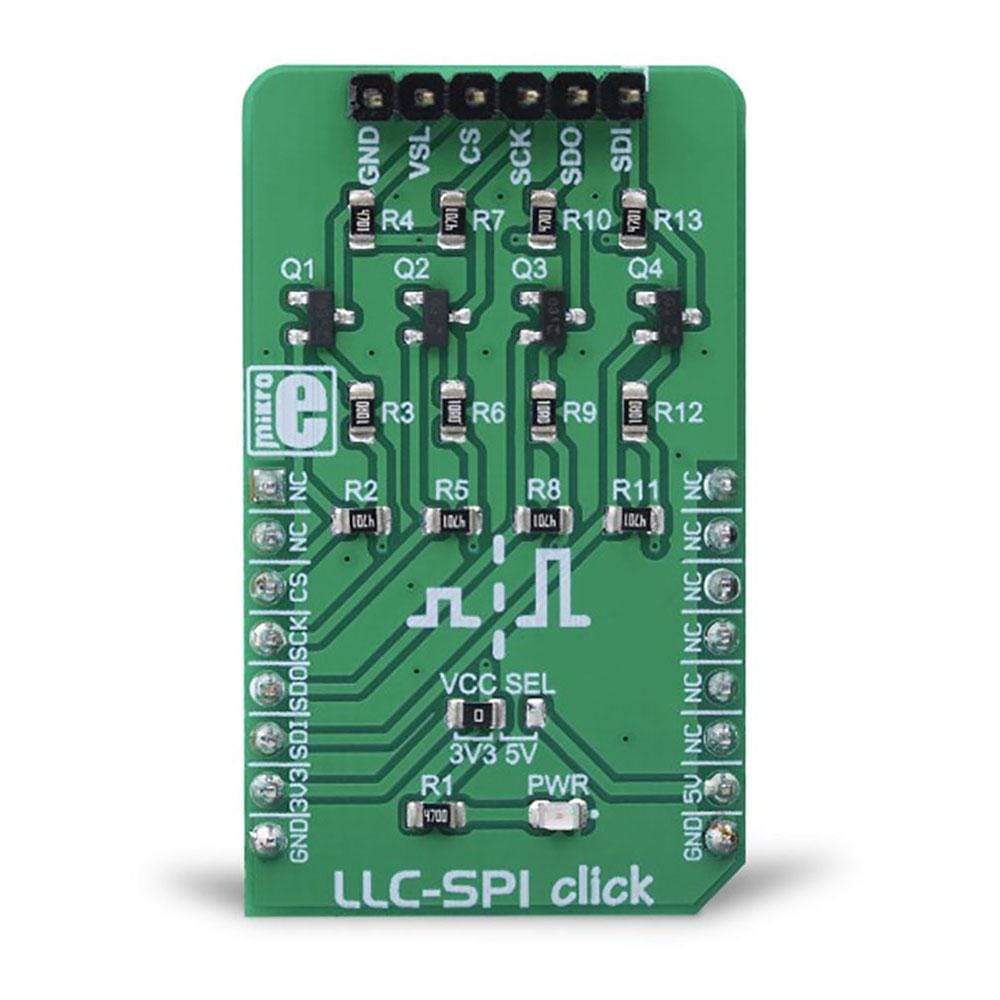
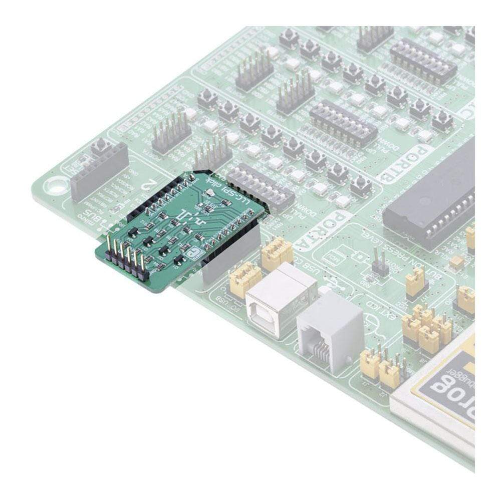
LLC-SPI Click Board™
LLC-SPI Click Board™
SKU: MIKROE-3298
Couldn't load pickup availability


Overview
The LLC SPI Click Board™ is a very useful Click Board™ that can be utilized as the level converter for logic signals. The topology of this logic level conversion (LLC) circuit is perfectly suited for SPI communication between devices with unmatched voltages of their logic signals. Although there are some specialised integrated circuits on the market, sometimes it is more convenient to have a simple solution made of just a few passive elements and four MOSFETs.
Downloads
Besides this, MOSFETs can withstand up to 20V across their terminals (12V VGS), and supports far greater currents than the typical ICs, making them less likely to fail. The LLC circuitry, also known as the level translator or level shifter, can be used in virtually any application that utilizes the SPI communication protocol and needs matching between logic voltage levels.
How Does The LLC I2C Click Board™ Work?
The LLC I2C Click Board™ does not use any integrated circuit, as already mentioned. With ICs avoided completely, there are some benefits gained: the overall cost of the LLC circuit is greatly reduced, a more robust MOSFET solution reduces the failure rate, and when powered off, both the low voltage and the high voltage sides are isolated from one another (by non-conductive MOSFETs). This type of circuit is sometimes referred to as a level shifting or level translating circuit and it is often necessary when one SPI device (typically a sensor IC) uses different logic voltage levels for the communication than the controller device, which is a microcontroller (MCU) in most cases. The conversion of this circuitry is bi-directional, which makes it suitable to be used with the SPI communication protocol.
The SPI protocol was first introduced by Motorola, in the '80s. The circuit is divided into low-side and high-side sections for future reference, however, both up-shifting, and down-shifting of the voltage level is possible. The mechanisms are slightly different, so each will be explained separately.
Up-shifting:
1. When there is a HIGH logic level on a low-side SPI line, both the gate and the source voltage of the MOSFET will be equal. This will turn OFF MOSFET since there is no gate-source voltage difference (e.g. VG=VS=VREF), while the pull-up resistor will pull the high-side SPI pins to a HIGH logic level.
2. When the low-side SPI line is driven to a LOW logic level, it will drive the source terminal of MOSFET to a LOW logic level, too. Since the gate is set to a fixed voltage value of the low-side voltage reference, a potential difference will form between the gate and the source terminal, causing the VGS voltage to appear. When this voltage raises above the gate threshold voltage (1.2V typically for the used transistors), the MOSFET will turn ON, conducting current through the high-side resistor, effectively bringing SPI pins on both low-side and high-side down to a LOW logic level.
Down-shifting:
1. When there is a HIGH logic level on a high-side SPI line, both the gate and the source voltage of the MOSFET will be equal, just like in the Up-shifting scenario.
2. When a high side SPI line is driven to a LOW logic level, it will drive the drain terminal of the MOSFET to a LOW logic level. Since the source of the MOSFET remains at the HIGH logic level (pulled up by a resistor), current will flow through the body diode of the MOSFET. In turn, the source-drain voltage (VSD) will drop towards the forward voltage of the MOSFET body diode. The lowered potential of the source terminal will result in forming the VGS voltage, ultimately turning ON MOSFET. From this moment, the MOSFET conducts the current, effectively bringing SPI pins on both low-side and high-side down to a LOW logic level. However, there is one condition in this case: the VGS voltage, which is equal to voltage of the low-side reference minus the forward voltage drop across the body diode, needs to be sufficient to allow turning MOSFET ON.
The reference voltage for the high-side can be selected by using the SMD jumper labelled as VCC SEL. The pull-up voltage for the high-side can be selected from the mikroBUS™ power rails, so it can be either 3.3V or 5V. For the low-side, an arbitrary reference voltage can be applied to the VSL pin of the J1 header, respecting the maximum voltage rating, as well as the condition mentioned above. J1 is the standard, 2.54mm pin-header. The low-side SPI related pins are also routed to the J1 header, allowing an external device to be connected (using the standard wire-jumpers). As already mentioned, the low-side can actually use higher voltage levels than the master, but in most usage scenarios, it will be lower than the master, thus the terminology used in the text above.
SPECIFICATIONS
| Type | Port expander |
| Applications | SPI logic level conversion circuit has its use in many different projects. It is used for the SPI logic voltage level matching between the host and the device |
| On-board modules | None |
| Key Features | Very low cost achieved using only passive elements, and four MOSFETs, ability to use an arbitrary voltage level conversion in the range from 1.2V up to 10V |
| Interface | SPI |
| Compatibility | mikroBUS |
| Click board size | M (42.9 x 25.4 mm) |
| Input Voltage | 3.3V or 5V |
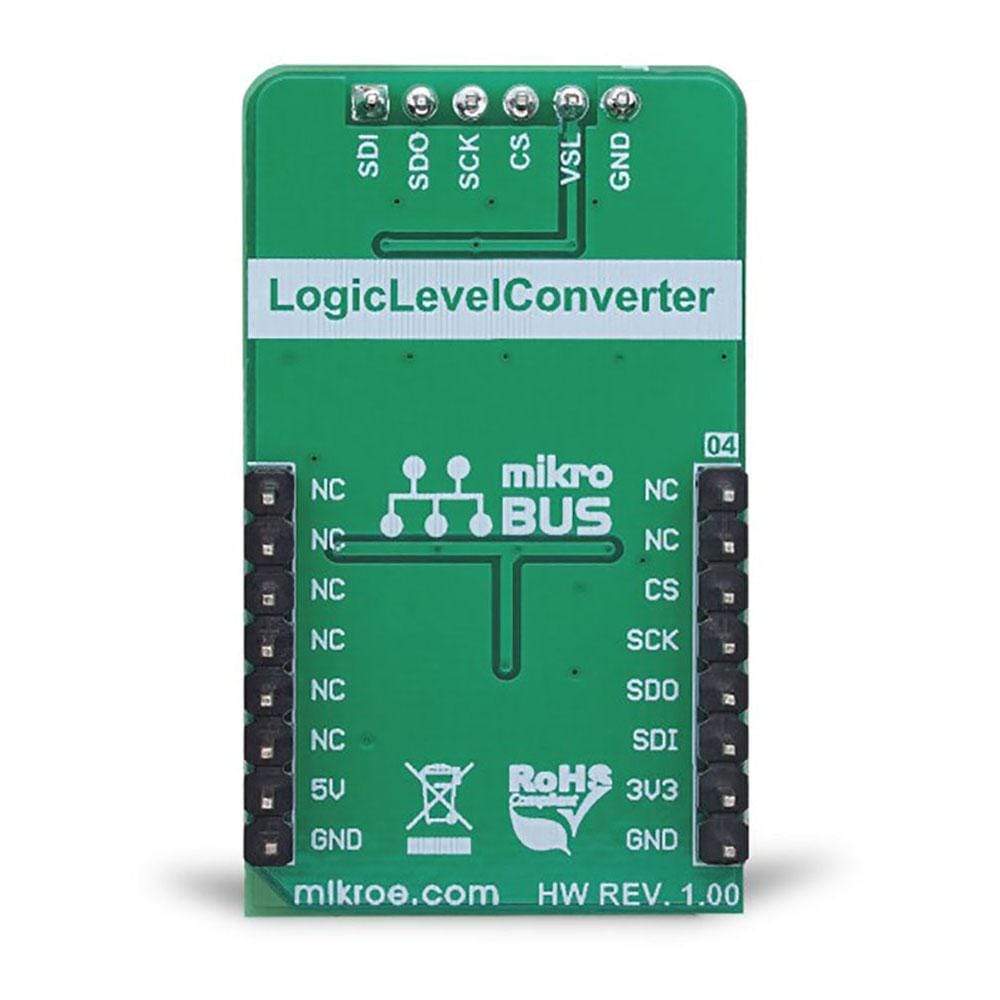
PINOUT DIAGRAM
This table shows how the pinout of the LLC I2C Click Board™ corresponds to the pinout on the mikroBUS™ socket (the latter shown in the two middle columns).
| Notes | Pin | Pin | Notes | ||||
|---|---|---|---|---|---|---|---|
| NC | 1 | AN | PWM | 16 | NC | ||
| NC | 2 | RST | INT | 15 | NC | ||
| SPI Chip Select | CS | 3 | CS | RX | 14 | NC | |
| SPI Clock | SCK | 4 | SCK | TX | 13 | NC | |
| SPI Data OUT | SDO | 5 | MISO | SCL | 12 | NC | |
| SPI Data IN | SDI | 6 | MOSI | SDA | 11 | NC | |
| Power supply | 3V3 | 7 | 3.3V | 5V | 10 | 5V | Power supply |
| Ground | GND | 8 | GND | GND | 9 | GND | Ground |
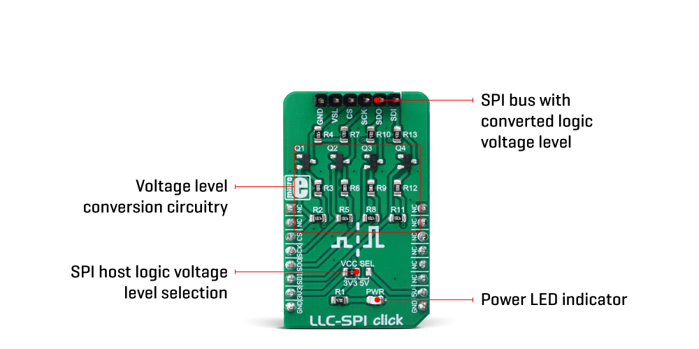
ONBOARD JUMPERS AND SETTINGS
| Label | Name | Default | Description |
|---|---|---|---|
| PWR | PWR | - | Power LED indicator |
| VCC SEL | VCC SEL | Left | SPI host logic voltage level selection: left position 3.3V, right position 5V |
| J1 | - | - | SPI bus with the converted voltage level |
| General Information | |
|---|---|
Part Number (SKU) |
MIKROE-3298
|
Manufacturer |
|
| Physical and Mechanical | |
Weight |
0.019 kg
|
| Other | |
EAN |
8606018714131
|
Frequently Asked Questions
Have a Question?
Be the first to ask a question about this.