


Mikroelektronika d.o.o.
I2C to SPI Click Board™
I2C to SPI Click Board™
SKU: MIKROE-3743
Couldn't load pickup availability
Overview
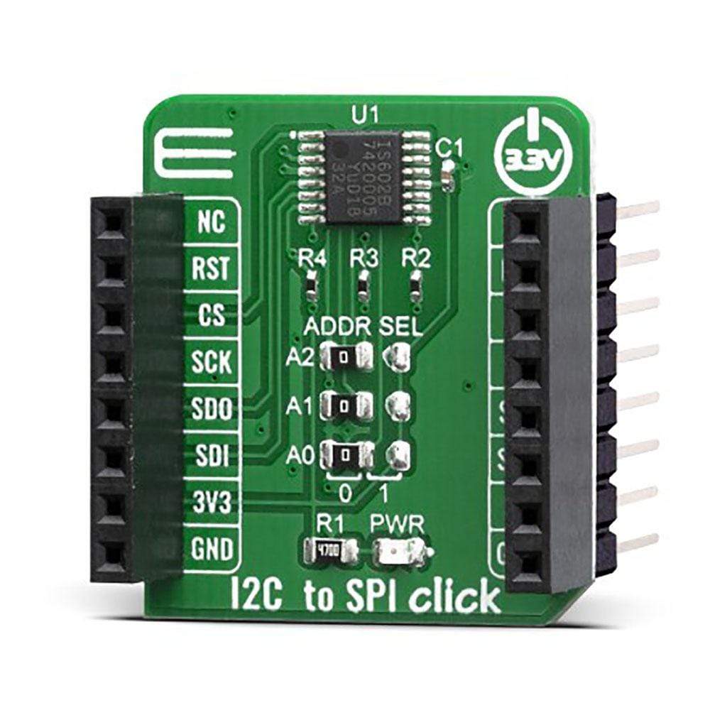
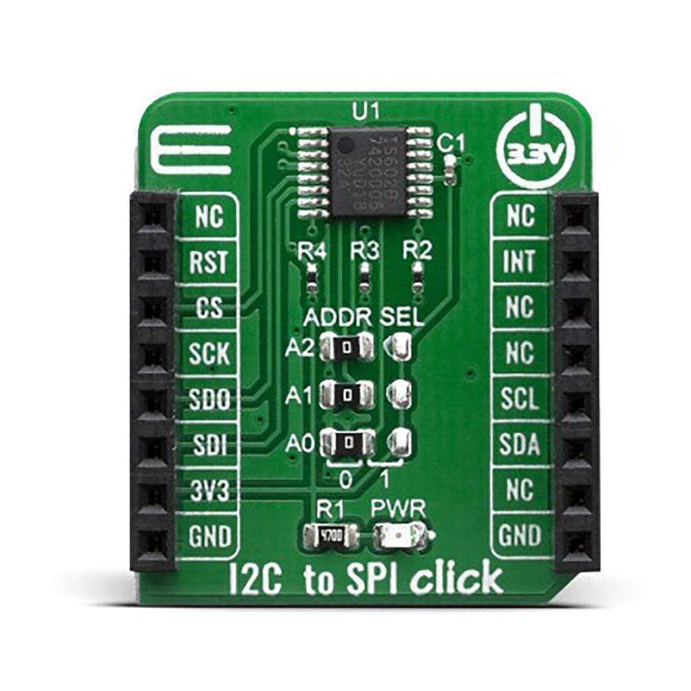
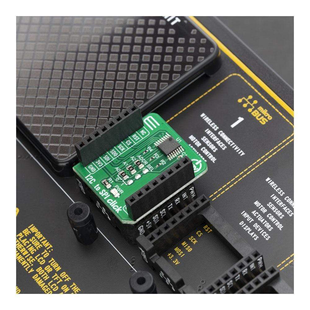
The I2C to SPI Click Board™ is an all-in-one solution that allows serving as an interface between a standard I2C-bus of a microcontroller and an SPI bus, which allows the microcontroller to communicate directly with SPI devices through its I2C-bus. It is equipped with stacking headers, so it can be easily connected. By offering an I2C-bus slave-transmitter or slave-receiver and an SPI master, this Click Board™ controls all the SPI bus-specific sequences, protocol, and timing. It also has its own internal oscillator, and it supports the SPI chip select output that may be configured as GPIO when not used.
The I2C to SPI Click Board™ is supported by a mikroSDK compliant library, which includes functions that simplify software development. This Click Board™ comes as a fully tested product, ready to be used on a system equipped with the mikroBUS™ socket.
Downloads
When it comes to communicating between chips on a printed circuit board, two protocols are extremely popular: Serial Peripheral Interface (SPI) and Inter-Integrated Circuit (IIC or I2C). They are both serial protocols with a shared bus supporting multiple devices, but they multiplex their lines very differently. However, both of them are extremely popular, as they are easy to implement, requiring few components and little code, over the other communication protocols. Both rely on serial communication to pass data and support multiple devices on one bus. Many microcontrollers, sensors, and peripherals rely on SPI and I2C to talk to each other. The I2C to SPI Click Board™ is a perfect solution for numerous needs, such as hand-held and portable equipment, PDAs, palmtops, digital cameras, and other devices that support I2C interface, offering the ability to communicate directly with SPI devices through its I2C-bus.
How Does The I2C to SPI Click Board™ Work?
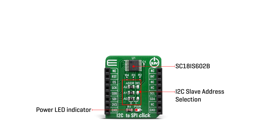
The design of the I2C to SPI Click Board™ is based around two SC18IS602B, an I2C-bus to SPI bridge from NXP. This IC bridges the data communication between the two interfaces, offering many additional features, such as the programmable I/O, internal oscillator option, active low interrupt output, low power mode, and more. The SC18IS602B operates as an I2C-bus slave-transmitter or slave-receiver and an SPI master. The SC18IS602B controls all the SPI bus-specific sequences, protocol, and timing. It also has its own internal oscillator, and it supports SPI chip select output that may be configured as GPIO when not used. This allows the software to be easily written or ported from another platform.
The I2C to SPI Click Board™ provides a byte-oriented I2C-bus interface that supports data transfers up to 400 kHz. When the I2C-bus master is reading data from the click board™, the device will be a slave-transmitter. It also can be a slave-receiver when the I2C-bus master is sending data. The SC18IS602B acts as an I2C-bus master at no time. However, it does have the ability to hold the SCL line LOW between bytes to complete its internal processes.
A slave address of the SC18IS602B is comprised of a fixed and a programmable part. The programmable part of the slave address enables the maximum possible number of such devices to be connected to the I2C-bus. Since the SC18IS602B has three programmable address bits (defined by the A2, A1, and A0 pins), it is possible to have eight of these devices on the same bus. Therefore, this Click board™ is equipped with three SMD jumpers, grouped under the ADDR SEL label, used to select the I2C slave address. By moving the jumpers at the desired position, the user can select the address used for the communication with the host MCU.
The #RESET pin performs the hardware reset of the SC18IS602B IC. The #RESET pin is routed to the mikroBUS™ RST pin and it is active LOW. The #INT allows the host MCU to receive an interrupt from the SC18IS602B IC. An interrupt is generated by the SC18IS602B after any SPI transmission has been completed. Therefore, the #INT of the SC18IS602B is routed to the INT pin of the mikroBUS™ socket. The interrupt can be cleared (INT pin HIGH) by sending a 'Clear Interrupt' command, although It is not necessary. This allows more optimized software (firmware) to be written, as the host MCU does not have to continuously poll the LSR register to see if any interrupt needs to be serviced.
The datasheet of the SC18IS602B offers more information about using and configuring the SC18IS602B IC. However, the Click board™ is supported by a mikroSDK library, offering functions that simplify the prototyping and firmware development.
The I2C to SPI Click Board™ is operated by 3.3V only. To be able to use it with MCUs that use 5V logic level on their communication lines, a proper level-translation circuit should be used.
SPECIFICATIONS
| Type | Port expander,RS232 |
| Applications | The I2C to SPI Click Board™ is a perfect solution for numerous needs, such as hand-held and portable equipment, PDAs, palmtops, digital cameras, and other devices that support I2C interface, offering the ability to communicate directly with SPI devices through its I2C-bus. |
| On-board modules | SC18IS602B, an I2C/SPI to UART interface, 64 bytes of transmit and receive FIFOs, and IrDA SIR built-in support, from NXP; MAX3237 IC, a low-power, true RS-232 transceiver, from Maxim Integrated |
| Key Features | It supports both I2C and SPI interfaces, bridging them to UART, supports a lot of other features including Line-Break generation and detection, programmable special character detection, auto flow control (software and hardware), 15kV ESD protection, onboard RS-232 connector, etc. |
| Interface | I2C,SPI,UART |
| Compatibility | mikroBUS |
| Click board size | S (28.6 x 25.4 mm) |
| Input Voltage | 3.3V |
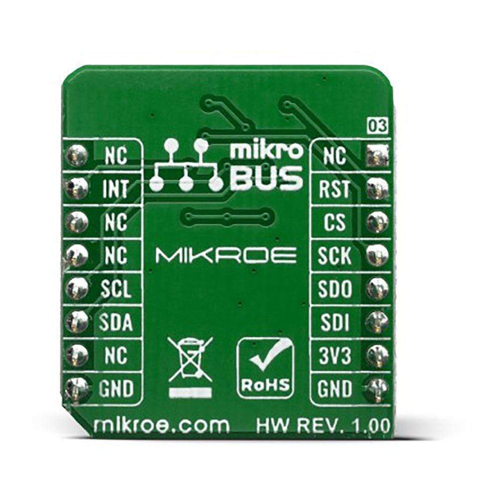
PINOUT DIAGRAM
This table shows how the pinout on the I2C to SPI Click Board™ corresponds to the pinout on the mikroBUS™ socket (the latter shown in the two middle columns).
| Notes | Pin | Pin | Notes | ||||
|---|---|---|---|---|---|---|---|
| NC | 1 | AN | PWM | 16 | NC | ||
| Reset | RST | 2 | RST | INT | 15 | INT | Interrupt |
| Chip Select / A0 | CS | 3 | CS | RX | 14 | NC | |
| SPI Clock | SCK | 4 | SCK | TX | 13 | NC | |
| SPI Data OUT | SDO | 5 | MISO | SCL | 12 | SCL | I2C Clock |
| SPI Data IN | SDI | 6 | MOSI | SDA | 11 | SDA | I2C Data |
| Power Supply | 3.3V | 7 | 3.3V | 5V | 10 | NC | |
| Ground | GND | 8 | GND | GND | 9 | GND | Ground |
ONBOARD SETTINGS AND INDICATORS
| Label | Name | Default | Description |
|---|---|---|---|
| LD1 | PWR | - | Power LED Indicator |
| JP1-JP3 | ADDR SELL | Left | Communication interface selection: left position 0, right position 1 |
| General Information | |
|---|---|
Part Number (SKU) |
MIKROE-3743
|
Manufacturer |
|
| Physical and Mechanical | |
Weight |
0.018 kg
|
| Other | |
EAN |
8606018716913
|
Frequently Asked Questions
Have a Question?
Be the first to ask a question about this.