


Mikroelektronika d.o.o.
PWM 2 Click-Platine
PWM 2 Click-Platine
SKU: MIKROE-3148
Verfügbarkeit für Abholungen konnte nicht geladen werden
Overview
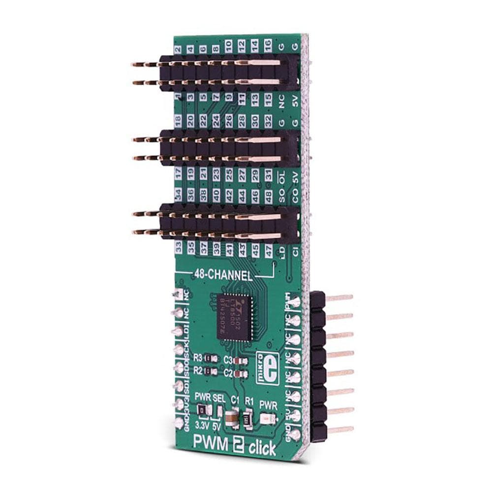
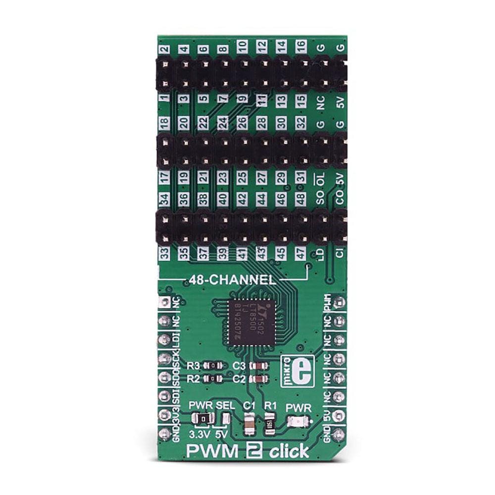
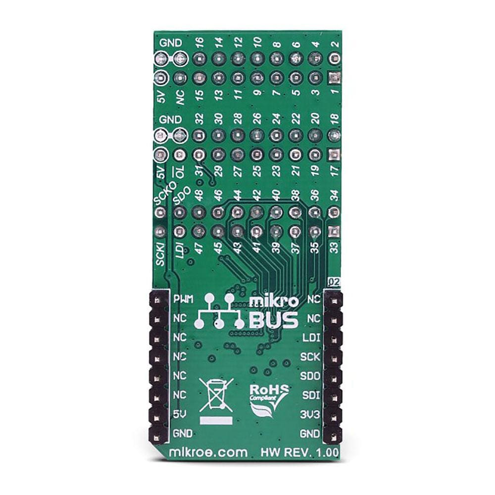
The PWM 2 Click Board™ offers 48 independently controlled PWM channels, available over the on-board headers, perfectly suited for driving LEDs. Each channel has a 12-bit PWM register associated to it, with the addition of the 6-bit correction register, also known as the dot correction register. PWM 2 is able to detect both synchronization errors and open LED errors, signaling the error via the dedicated pin and the status frame.
The PWM 2 Click Board™ fully supports cascading, exposing all the necessary pins on the on-board headers, so it can support a large array of LED elements.
Downloads
Das PWM 2 Click Board™ bietet 48 unabhängig gesteuerte PWM-Kanäle, die über die integrierten Stiftleisten verfügbar sind und sich perfekt zum Ansteuern von LEDs eignen. Jedem Kanal ist ein 12-Bit-PWM-Register zugeordnet, zusätzlich gibt es ein 6-Bit-Korrekturregister, auch als Punktkorrekturregister bekannt. PWM 2 kann sowohl Synchronisierungsfehler als auch offene LED-Fehler erkennen und signalisiert den Fehler über den dedizierten Pin und den Statusrahmen.
Das PWM 2 Click Board™ unterstützt die Kaskadierung vollständig und stellt alle notwendigen Pins auf den integrierten Headern bereit, sodass es eine große Anzahl von LED-Elementen unterstützen kann.
| General Information | |
|---|---|
Part Number (SKU) |
MIKROE-3148
|
Manufacturer |
|
| Physical and Mechanical | |
Weight |
0.03 kg
|
| Other | |
EAN |
8606018713493
|
Frequently Asked Questions
Have a Question?
Be the first to ask a question about this.