


Mikroelektronika d.o.o.
Flash 8 Click-Platine
Flash 8 Click-Platine
SKU: MIKROE-5293
Verfügbarkeit für Abholungen konnte nicht geladen werden


Key Features
Overview
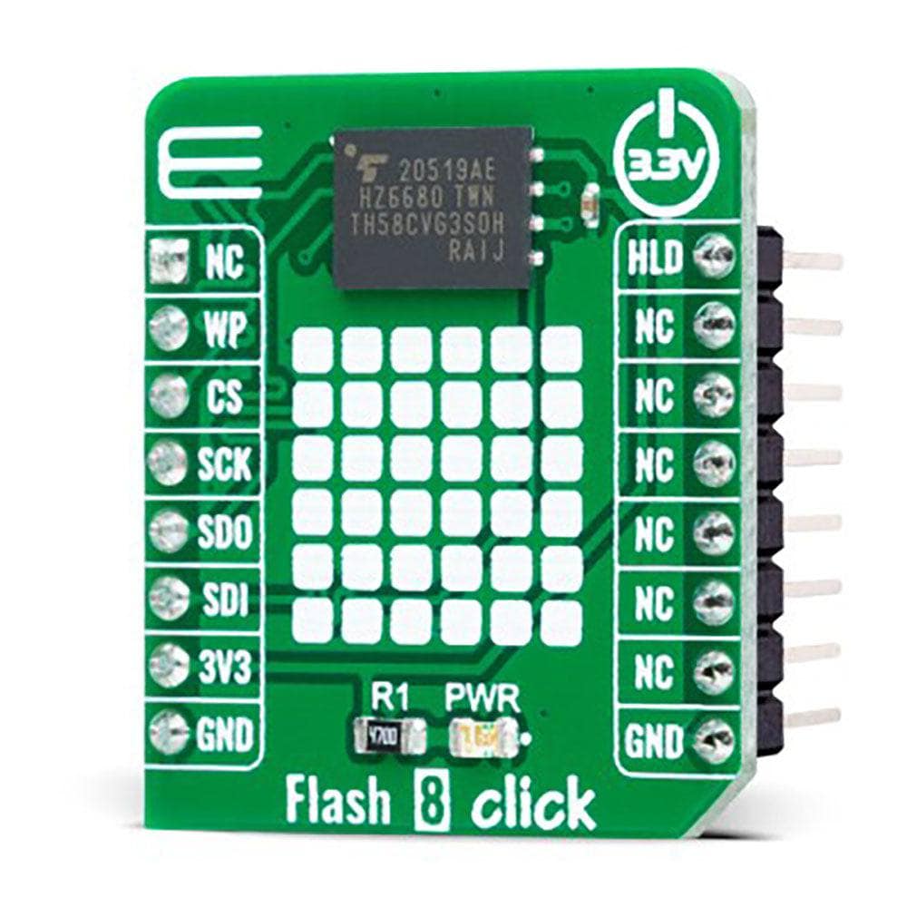
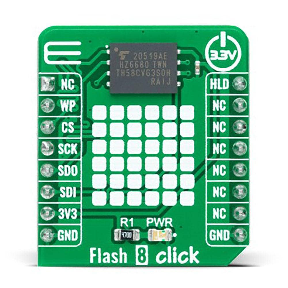
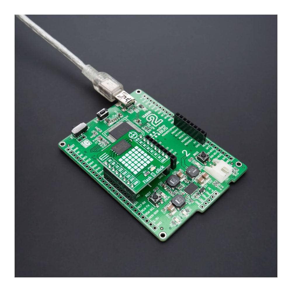
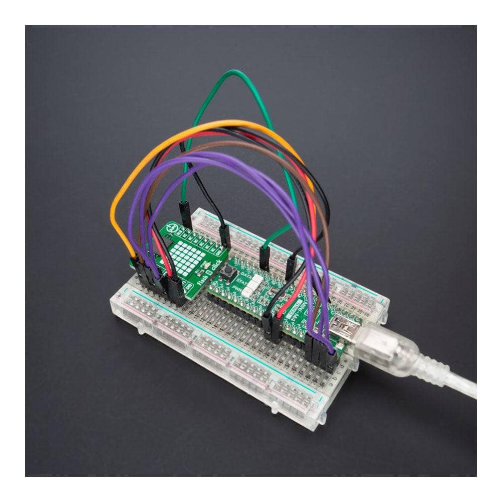
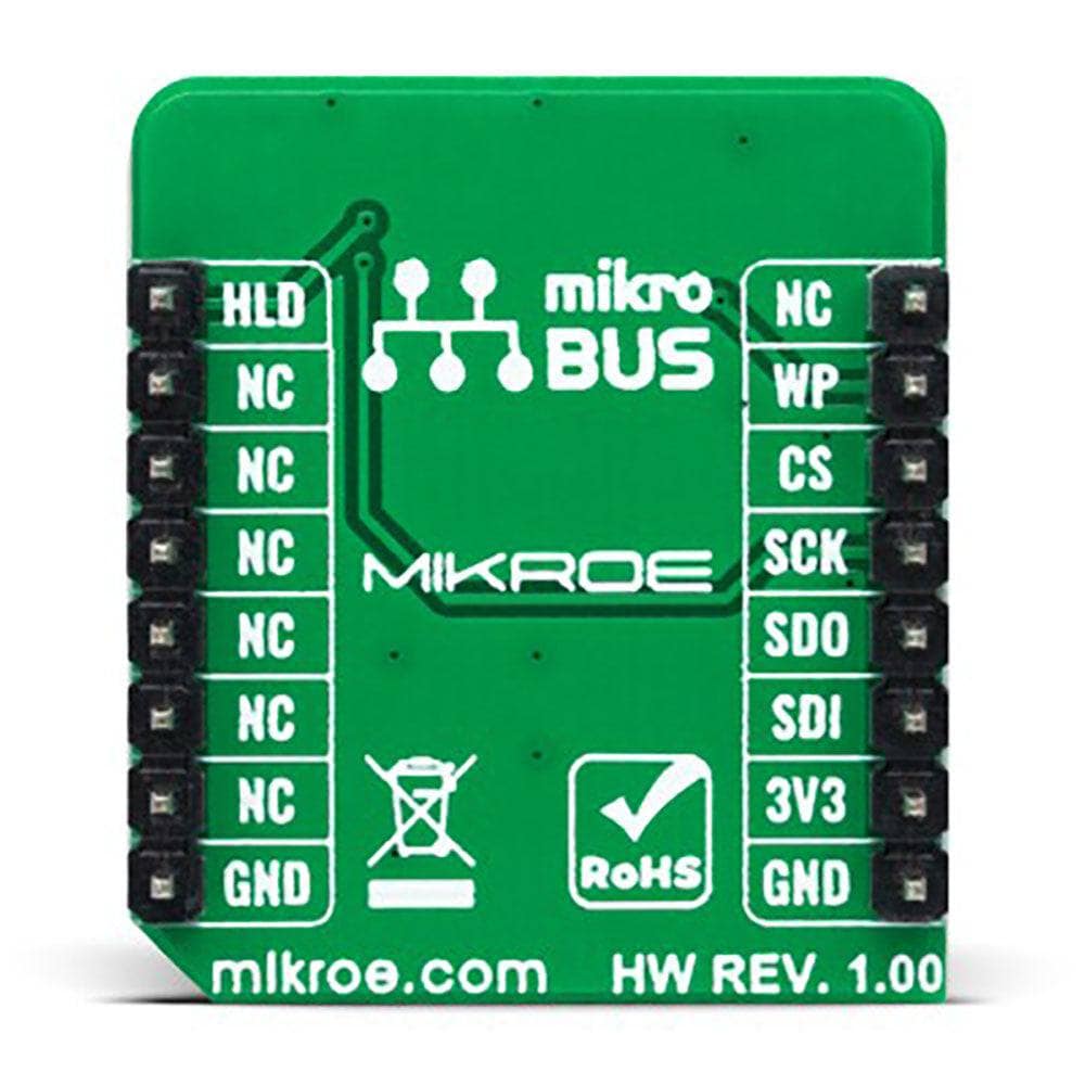
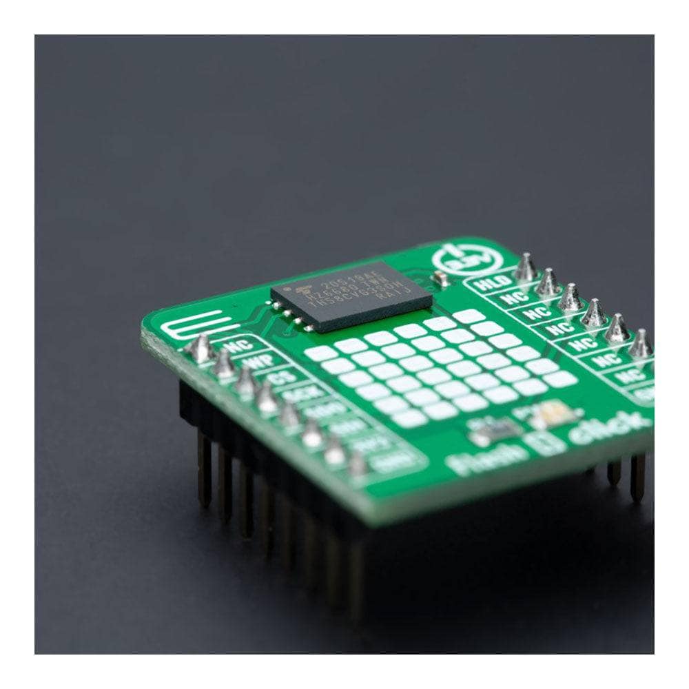
The Flash 8 Click Board™ is a compact add-on board representing a highly reliable memory solution. This board features the GD5F2GQ5UEYIGR, a 2Gb high-density non-volatile memory storage solution for embedded systems from GigaDevice Semiconductor. It is based on an industry-standard NAND Flash memory core, representing an attractive alternative to SPI-NOR and standard parallel NAND Flash with advanced features. The GD5F2GQ5UEYIGR also has advanced security features (8K-Byte OTP region), software/hardware write protection, can withstand many write cycles (minimum 100k), and has a data retention period greater than ten years. This Click board™ is suitable for storage and data transfer in consumer devices and industrial applications.
The Flash 8 Click Board™ is supported by a mikroSDK compliant library, which includes functions that simplify software development. This Click board™ comes as a thoroughly tested product, ready to be used on a system equipped with the mikroBUS™ socket.
Downloads
Das Flash 8 Click Board™ ist eine kompakte Zusatzplatine, die eine äußerst zuverlässige Speicherlösung darstellt. Diese Platine verfügt über das GD5F2GQ5UEYIGR , eine 2 GB-Speicherlösung mit hoher Dichte und nichtflüchtigem Speicher für eingebettete Systeme von GigaDevice Semiconductor. Es basiert auf einem NAND-Flash-Speicherkern nach Industriestandard und stellt eine attraktive Alternative zu SPI-NOR und standardmäßigem parallelem NAND-Flash mit erweiterten Funktionen dar. Das GD5F2GQ5UEYIGR verfügt außerdem über erweiterte Sicherheitsfunktionen (8 KB OTP-Region), Software-/Hardware-Schreibschutz, hält vielen Schreibzyklen stand (mindestens 100 KB) und hat eine Datenaufbewahrungsdauer von mehr als zehn Jahren. Dieses Click Board™ ist für die Speicherung und Datenübertragung in Verbrauchergeräten und industriellen Anwendungen geeignet.
Das Flash 8 Click Board™ wird von einer mikroSDK-kompatiblen Bibliothek unterstützt, die Funktionen enthält, die die Softwareentwicklung vereinfachen. Dieses Click Board™ ist ein gründlich getestetes Produkt und kann auf einem System verwendet werden, das mit der mikroBUS™-Buchse ausgestattet ist.
| General Information | |
|---|---|
Part Number (SKU) |
MIKROE-5293
|
Manufacturer |
|
| Physical and Mechanical | |
Weight |
0.02 kg
|
| Other | |
EAN |
8606027387890
|
Frequently Asked Questions
Have a Question?
Be the first to ask a question about this.