

Mikroelektronika d.o.o.
ADC 15 Click-Platine
ADC 15 Click-Platine
SKU: MIKROE-4890
Verfügbarkeit für Abholungen konnte nicht geladen werden


Key Features
Overview
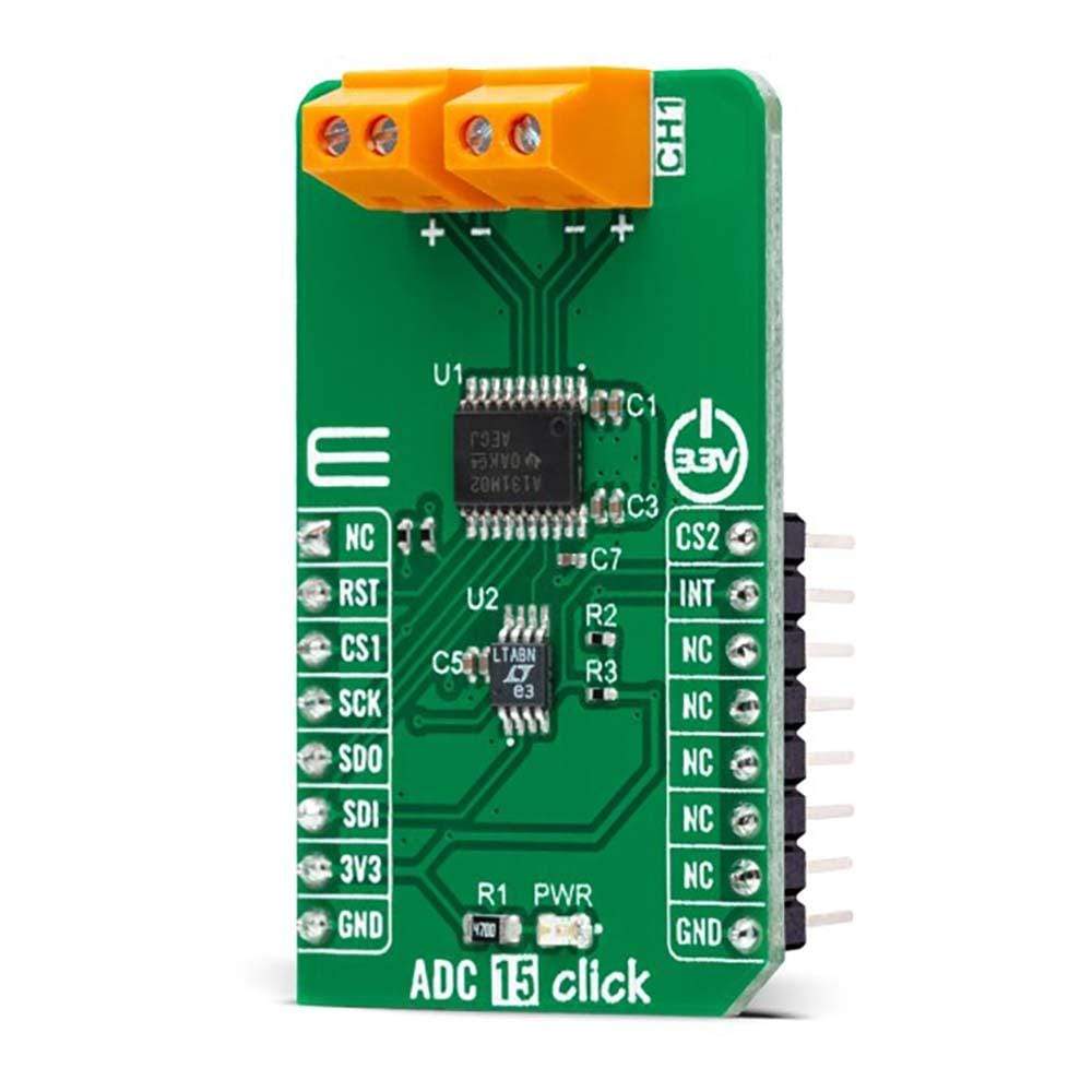
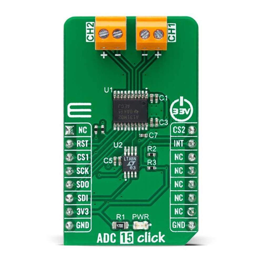
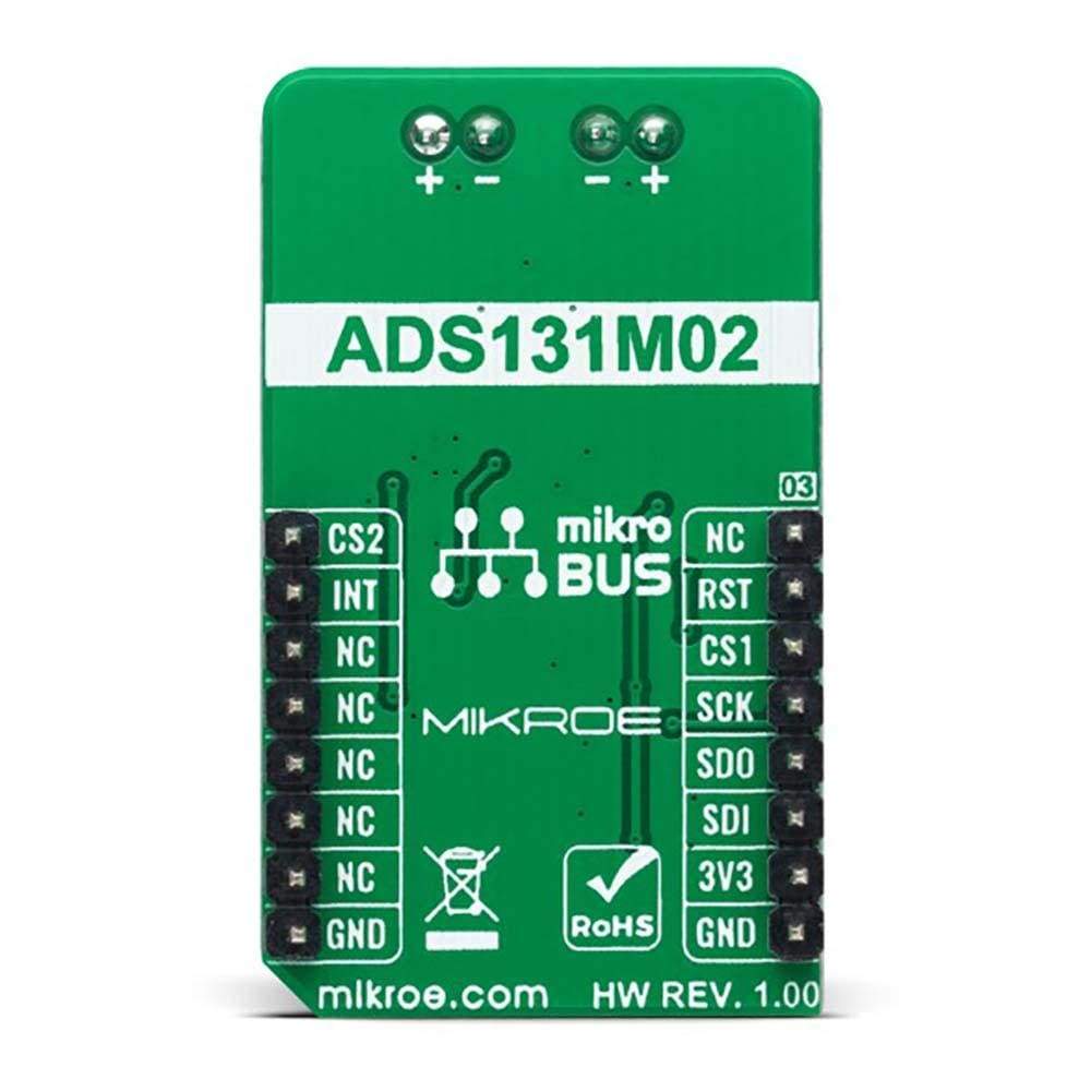
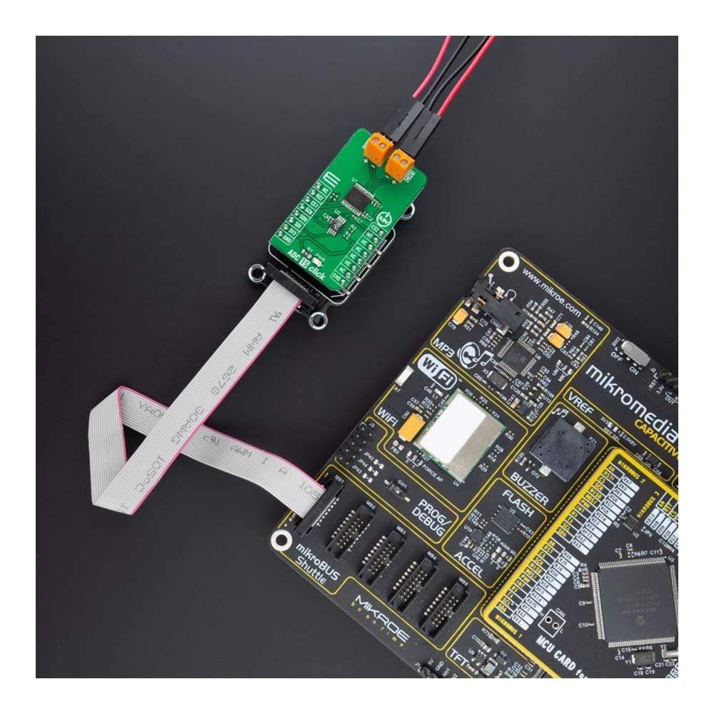
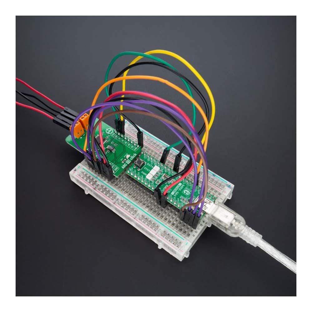
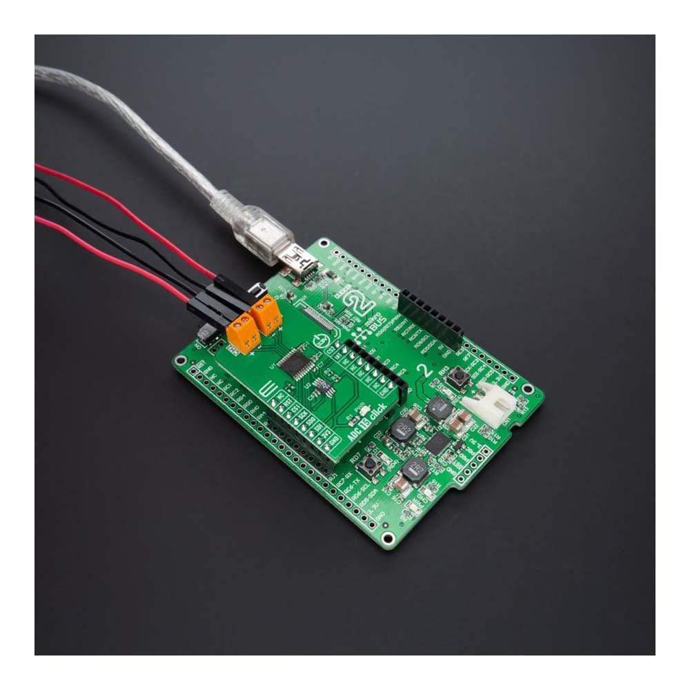
The ADC 15 Click Board™ is a compact add-on board that contains a high-performance data converter. This board features the ADS131M02, a two-channel, simultaneously sampling, 24-bit, delta-sigma (ΔΣ), analogue-to-digital converter from Texas Instruments. The ADC inputs can be independently configured via serial peripheral interface depending on the sensor input. A low noise, programmable gain amplifier (PGA) provides gains ranging from 1 to 128 to amplify low-level signals. Additionally, this ADC integrates channel-to-channel phase, offset and gain calibration registers to help remove signal-chain errors alongside a low-drift, 1.2V integrated reference.
The ADC 15 Click Board™ offers a wide dynamic range, low power, and energy-measurement-specific features, making the device an excellent fit for energy metering, power metrology, and circuit breaker applications.
Downloads
Der ADC 15 Click Board™ ist eine kompakte Zusatzplatine, die einen Hochleistungsdatenkonverter enthält. Diese Platine verfügt über den ADS131M02, einen zweikanaligen, gleichzeitig abtastenden, 24-Bit-Delta-Sigma-(ΔΣ)-Analog-Digital-Konverter von Texas Instruments. Die ADC-Eingänge können je nach Sensoreingang unabhängig über die serielle Peripherieschnittstelle konfiguriert werden. Ein rauscharmer, programmierbarer Verstärkungsverstärker (PGA) bietet Verstärkungen von 1 bis 128, um Signale mit niedrigem Pegel zu verstärken. Darüber hinaus integriert dieser ADC Kanal-zu-Kanal-Phasen-, Offset- und Verstärkungskalibrierungsregister, um Signalkettenfehler neben einer driftarmen, integrierten 1,2-V-Referenz zu beseitigen.
Das ADC 15 Click Board™ bietet einen großen Dynamikbereich, einen niedrigen Stromverbrauch und energiemessungsspezifische Funktionen, wodurch sich das Gerät hervorragend für Anwendungen in den Bereichen Energiemessung, Leistungsmesstechnik und Leistungsschalter eignet.
| General Information | |
|---|---|
Part Number (SKU) |
MIKROE-4890
|
Manufacturer |
|
| Physical and Mechanical | |
Weight |
0.02 kg
|
| Other | |
EAN |
8606027384356
|
Frequently Asked Questions
Have a Question?
Be the first to ask a question about this.