


Mikroelektronika d.o.o.
Clock Gen Click-Platine
Clock Gen Click-Platine
SKU: MIKROE-4113
Verfügbarkeit für Abholungen konnte nicht geladen werden


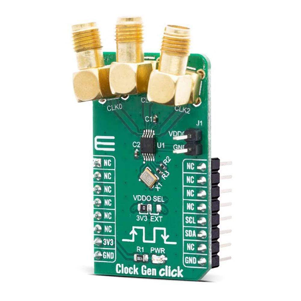
Overview
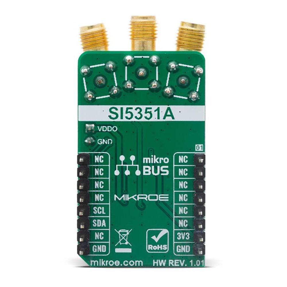
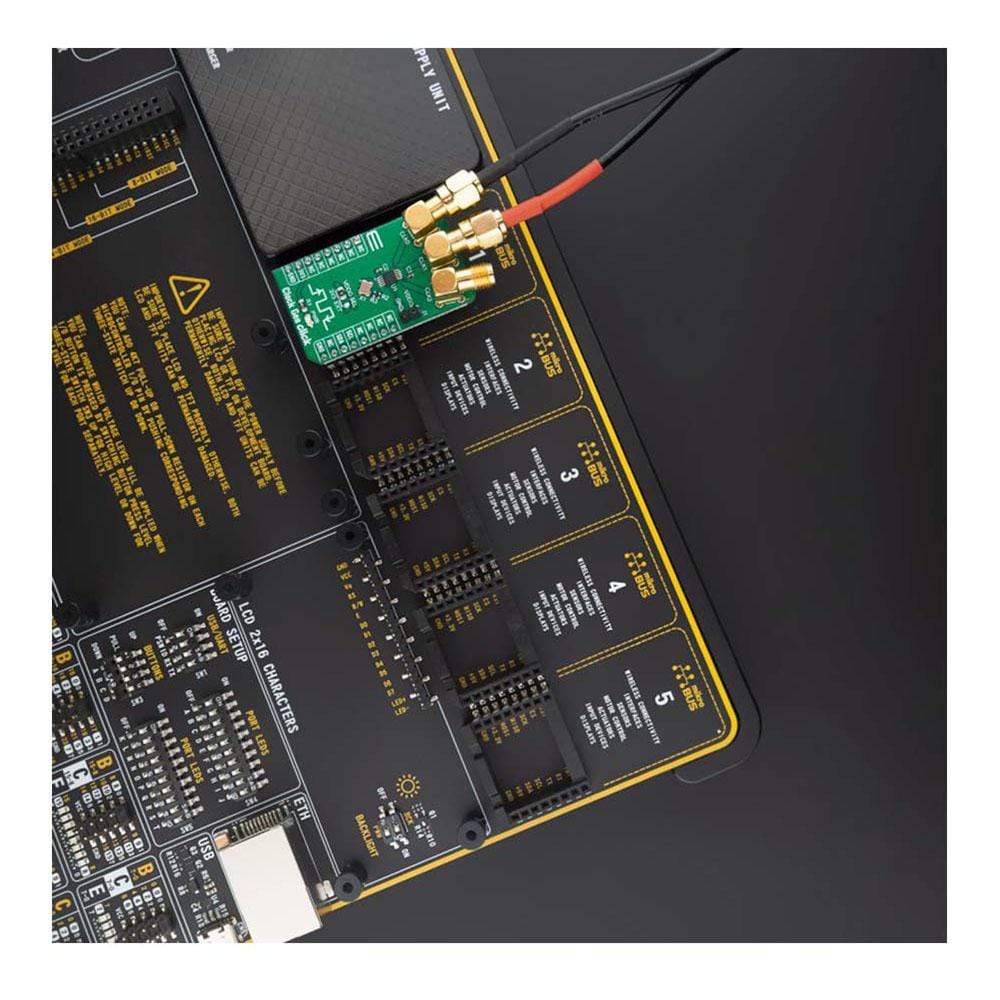
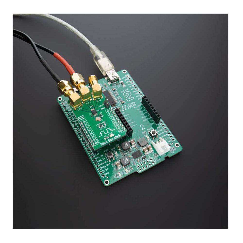
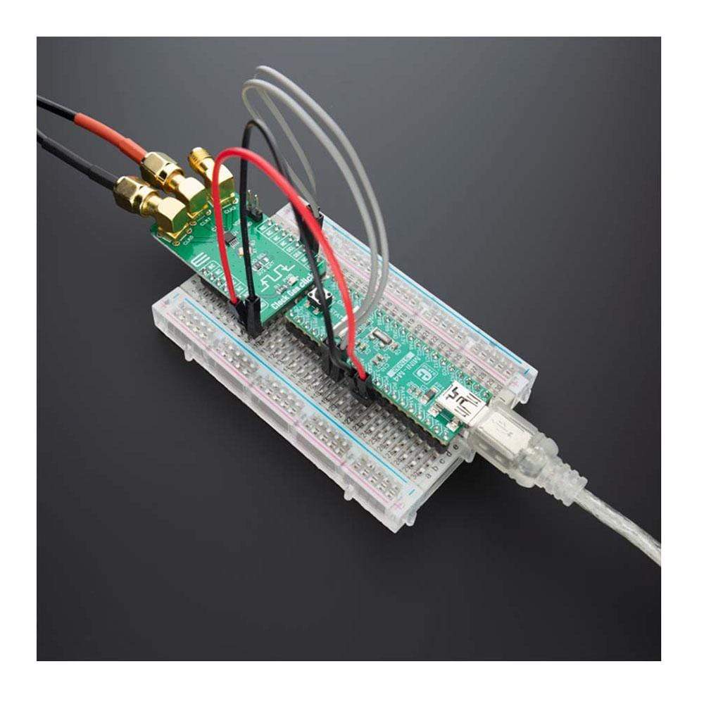
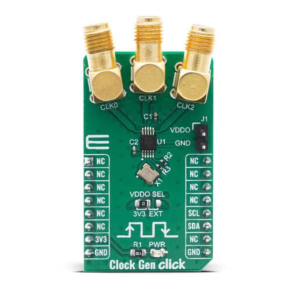
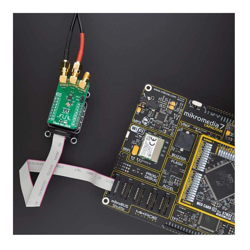
The Clock Gen Click Board™ offers an ideal replacement for crystals, crystal oscillators, VCXOs, phase-locked loops (PLLs), and fanout buffers in cost-sensitive applications. This Click Board™ features the Si5351A from Silicon Labs, an I2C configurable clock generator based on a PLL + high-resolution MultiSynth fractional divider architecture which can generate any frequency up to 200 MHz on each of its outputs with 0 ppm error.
The Si5351A is capable of generating synchronous or free-running non-integer related clock frequencies at each of its outputs (CLK0, CLK1, and CLK2), enabling one device to synthesize clocks for multiple clock domains in a design. It eliminates the need for higher cost, custom pullable crystals while providing reliable operation over a wide tuning range. The Si5351C offers the same flexibility but synchronizes to an external reference clock.
Downloads
Das Clock Gen Click Board™ bietet einen idealen Ersatz für Kristalle, Kristalloszillatoren, VCXOs, Phasenregelschleifen (PLLs) und Fanout-Puffer in kostensensiblen Anwendungen. Dieses Click Board™ verfügt über den Si5351A von Silicon Labs, einen I2C-konfigurierbaren Taktgenerator basierend auf einer PLL + hochauflösenden MultiSynth-Fraktionsteilerarchitektur, die an jedem ihrer Ausgänge jede Frequenz bis zu 200 MHz mit 0 ppm Fehler erzeugen kann.
Der Si5351A kann an jedem seiner Ausgänge (CLK0, CLK1 und CLK2) synchrone oder freilaufende, nicht ganzzahlige Taktfrequenzen erzeugen, sodass ein Gerät Takte für mehrere Taktdomänen in einem Design synthetisieren kann. Es macht teurere, individuell ziehbare Kristalle überflüssig und bietet gleichzeitig einen zuverlässigen Betrieb über einen weiten Abstimmungsbereich. Der Si5351C bietet dieselbe Flexibilität, synchronisiert sich jedoch mit einem externen Referenztakt.
| General Information | |
|---|---|
Part Number (SKU) |
MIKROE-4113
|
Manufacturer |
|
| Physical and Mechanical | |
Weight |
0.021 kg
|
| Other | |
EAN |
8606018717439
|
Frequently Asked Questions
Have a Question?
Be the first to ask a question about this.