

Mikroelektronika d.o.o.
Scanner Click-Platine
Scanner Click-Platine
SKU: MIKROE-4108
Verfügbarkeit für Abholungen konnte nicht geladen werden


Overview
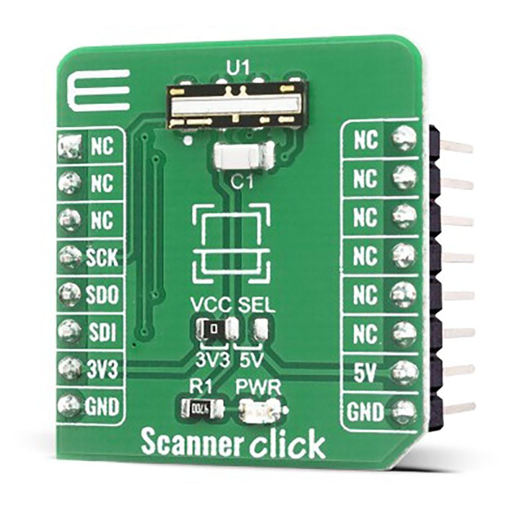
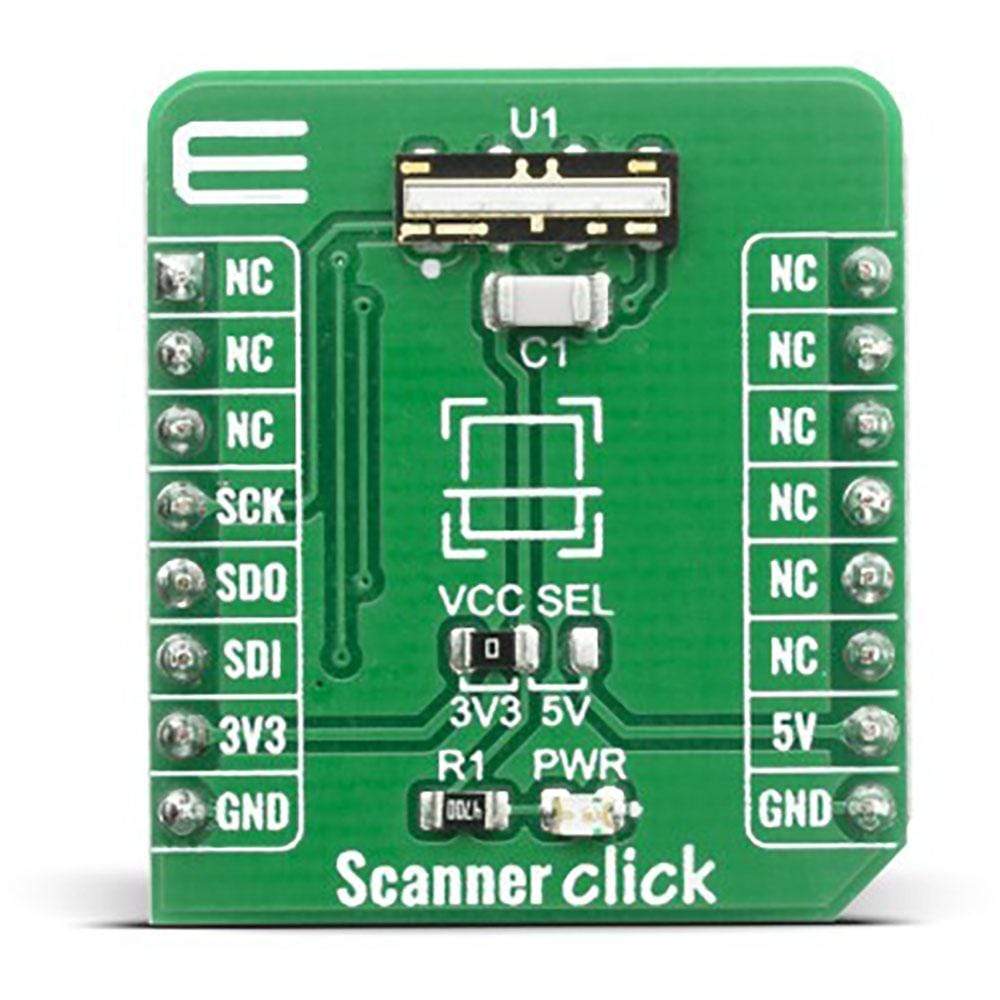
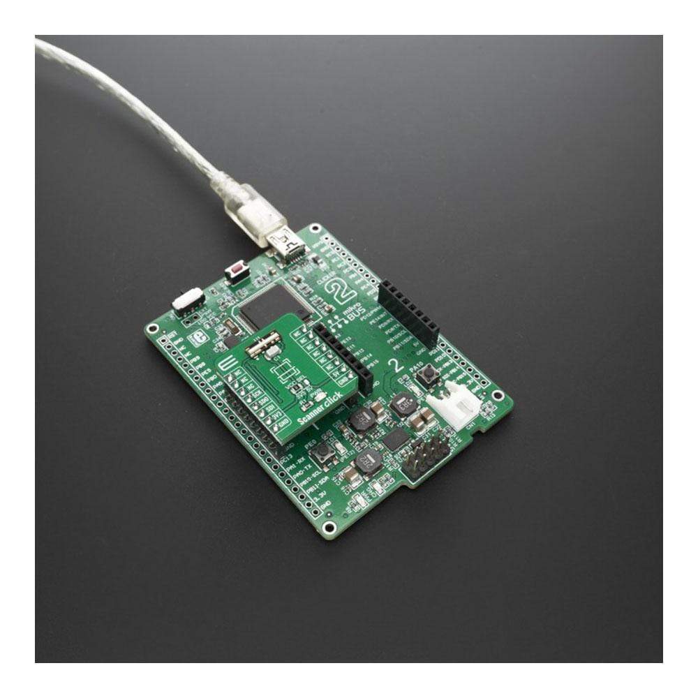
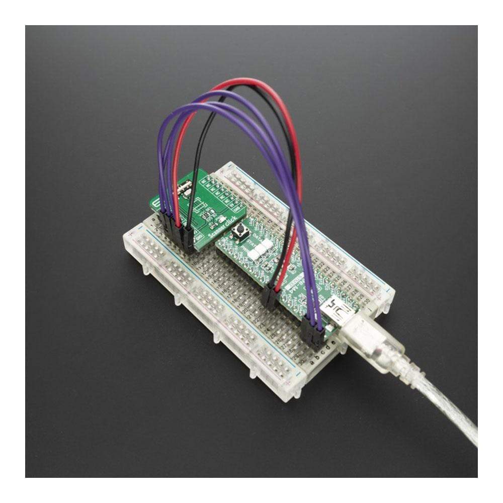
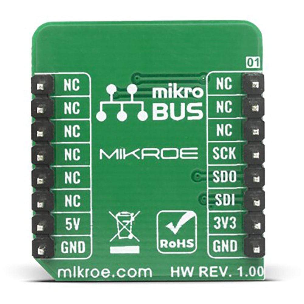
The Scanner Click Board™ is an optical scanner expansion board for building optical cost-sensitive scanners and printers. The main component of this board is a 102 pixels linear optical array sensor marked TSL3301CL from AMS. For accessing sensor registers from any host controller communication is accomplished through a three-wire SPI high-speed serial interface. This linear optical sensor provides high-density pixel count and integrated analogue-to-digital conversion to the Scanner Click Board™ and also enables high-resolution scanning and scalable operating range. This Click Board™ is most suitable for the applications like scanners, printer edge detects and optical character recognition.
The Scanner Click Board™ is supported by a mikroSDK compliant library, which includes functions that simplify software development. This Click Board™ comes as a fully tested product, ready to be used on a system equipped with the mikroBUS™ socket.
Downloads
Das Scanner Click Board™ ist eine optische Scanner-Erweiterungskarte zum Bau kostensensibler optischer Scanner und Drucker. Die Hauptkomponente dieser Karte ist ein linearer optischer Array-Sensor mit 102 Pixeln mit der Bezeichnung TSL3301CL von AMS. Für den Zugriff auf Sensorregister von jedem Host-Controller aus erfolgt die Kommunikation über eine dreiadrige SPI-Hochgeschwindigkeits-Seriellschnittstelle. Dieser lineare optische Sensor bietet eine hohe Pixeldichte und eine integrierte Analog-Digital-Umwandlung für das Scanner Click Board™ und ermöglicht außerdem hochauflösendes Scannen und einen skalierbaren Betriebsbereich. Dieses Click Board™ ist am besten für Anwendungen wie Scanner, Druckerkantenerkennung und optische Zeichenerkennung geeignet.
Das Scanner Click Board™ wird von einer mikroSDK-kompatiblen Bibliothek unterstützt, die Funktionen enthält, die die Softwareentwicklung vereinfachen. Dieses Click Board™ wird als vollständig getestetes Produkt geliefert und ist bereit für den Einsatz auf einem System, das mit der mikroBUS™-Buchse ausgestattet ist.
| General Information | |
|---|---|
Part Number (SKU) |
MIKROE-4108
|
Manufacturer |
|
| Physical and Mechanical | |
Weight |
0.02 kg
|
| Other | |
EAN |
8606018717552
|
Frequently Asked Questions
Have a Question?
Be the first to ask a question about this.