


Mikroelektronika d.o.o.
Step Up Klickbrett
Step Up Klickbrett
SKU: MIKROE-3709
Verfügbarkeit für Abholungen konnte nicht geladen werden
Overview
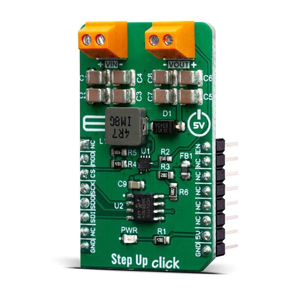
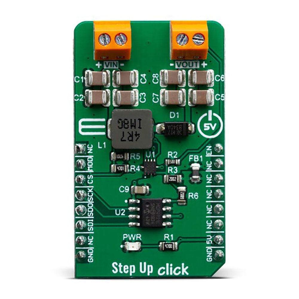
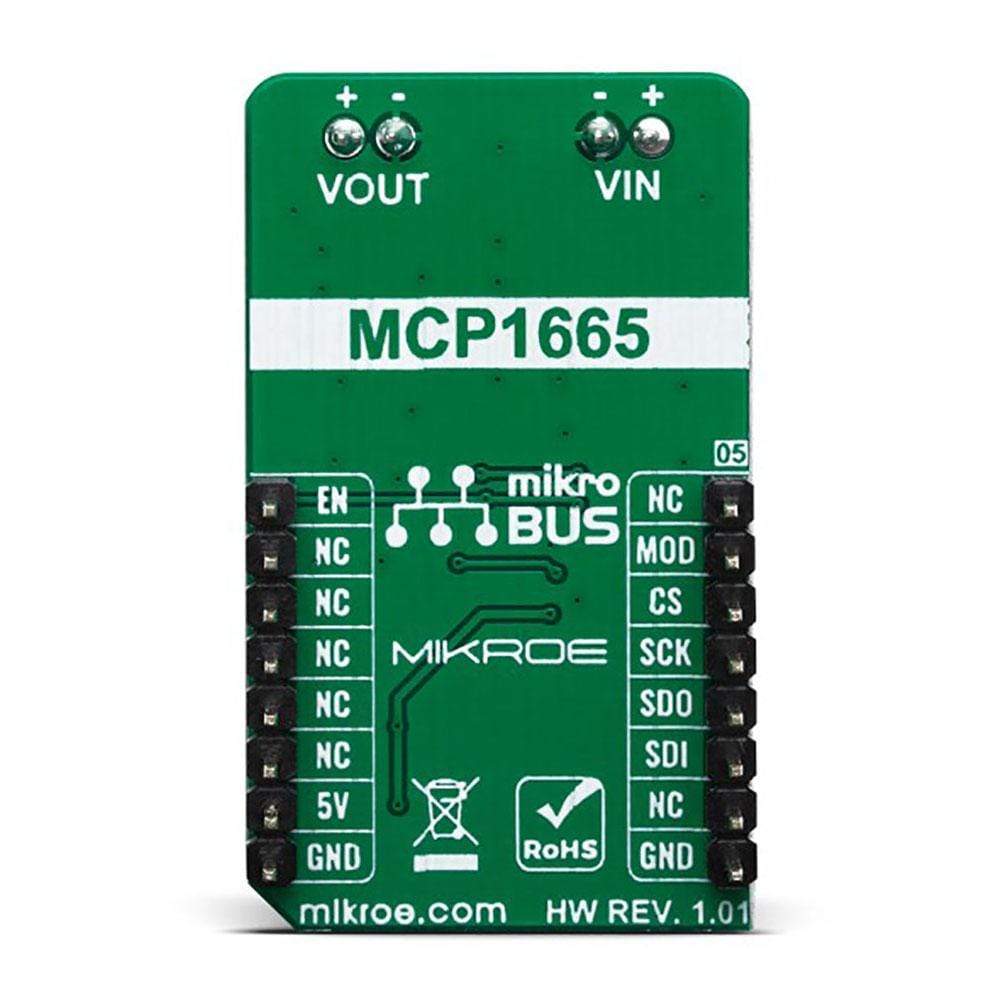
The Step Up Click Board™ is a fixed frequency DC-DC step-up (boost) regulator, which can be obtained from any low voltage input - such as NiCd, NiMH or one cell Li-Po/Li-Ion batteries. This click features very high efficiency, low noise and anti-ringing voltage output and inrush current limiting with the internal soft-start, as well as true disconnect option for minimized power drain, when in shutdown mode. These features allow this device to be used as the power source for various battery-operated devices, such as microcontrollers, various portable embedded electronic devices, handheld instruments, GPS modules, or various battery-operated USB emergency backup chargers. Very good switching efficiency factor ensures prolonged battery life for any application this device is used in.
The Step Up Click Board™ is supported by a mikroSDK compliant library, which includes functions that simplify software development. This Click Board™ comes as a fully tested product, ready to be used on a system equipped with the mikroBUS™ socket.
Downloads
Das Step Up Click Board™ ist ein DC-DC-Aufwärtsregler (Boost-Regler) mit fester Frequenz, der von jedem Niederspannungseingang bezogen werden kann – wie NiCd-, NiMH- oder einzelligen Li-Po/Li-Ion-Akkus. Dieses Click bietet einen sehr hohen Wirkungsgrad, geringes Rauschen und eine Anti-Ringing-Spannungsausgabe sowie eine Einschaltstrombegrenzung mit internem Softstart sowie eine echte Trennoption für minimalen Stromverbrauch im Abschaltmodus. Diese Funktionen ermöglichen die Verwendung dieses Geräts als Stromquelle für verschiedene batteriebetriebene Geräte wie Mikrocontroller, verschiedene tragbare eingebettete elektronische Geräte, Handgeräte, GPS-Module oder verschiedene batteriebetriebene USB-Notfall-Backup-Ladegeräte. Ein sehr guter Schaltwirkungsgrad sorgt für eine verlängerte Batterielebensdauer für jede Anwendung, in der dieses Gerät verwendet wird.
Das Step Up Click Board™ wird von einer mikroSDK-kompatiblen Bibliothek unterstützt, die Funktionen enthält, die die Softwareentwicklung vereinfachen. Dieses Click Board™ wird als vollständig getestetes Produkt geliefert und ist bereit für den Einsatz auf einem System, das mit der mikroBUS™-Buchse ausgestattet ist.
| General Information | |
|---|---|
Part Number (SKU) |
MIKROE-3709
|
Manufacturer |
|
| Physical and Mechanical | |
Weight |
0.021 kg
|
| Other | |
EAN |
8606018716678
|
Frequently Asked Questions
Have a Question?
Be the first to ask a question about this.