EEPROM 2 Click-Platine
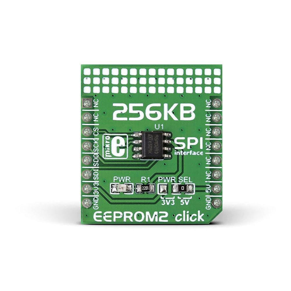
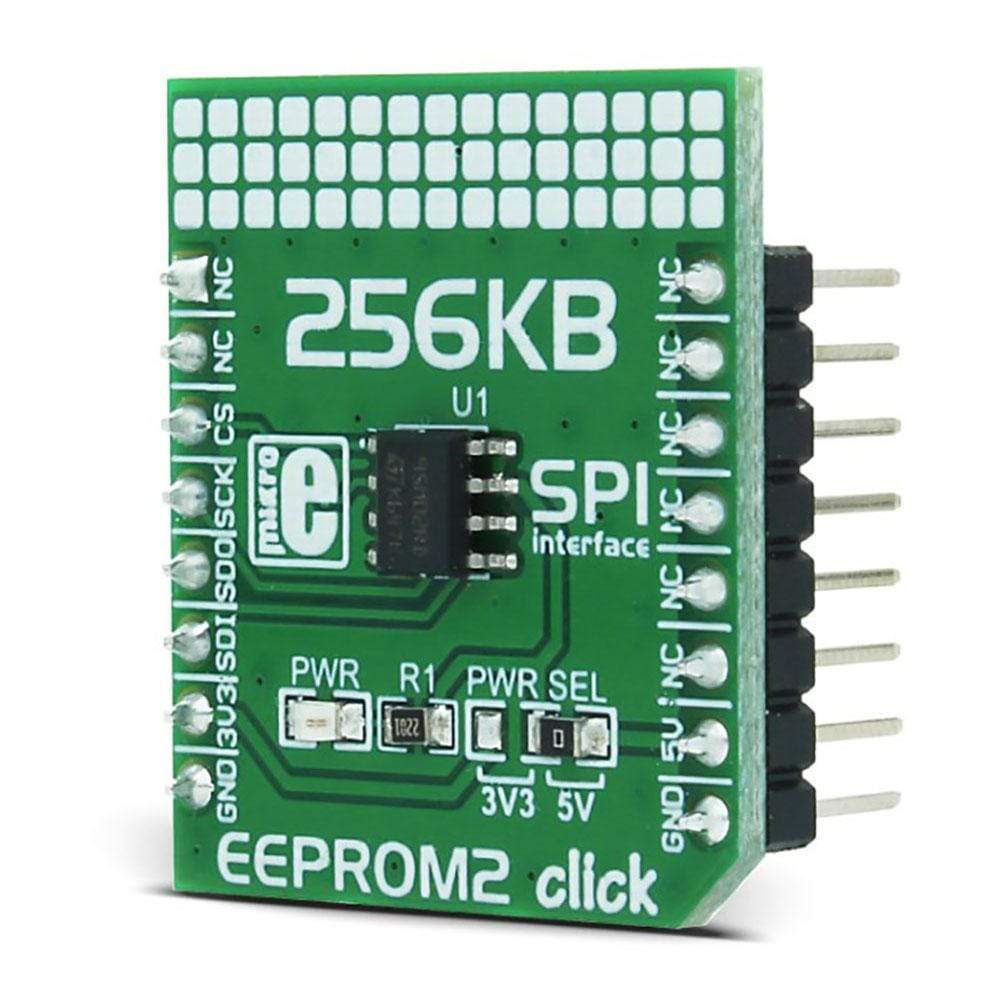
Das EEPROM 2 Click Board™ enthält den M95M02-DR DIP-8-Sockel-EEPROM-Chip von ST mit 256 KB Speicher. Der Chip hat Byte- und Seitenschreibgeschwindigkeiten von höchstens 10 ms.
The EEPROM2 Click Board™ provides 2 Mbit (2,097,152 bits) of Electrically Erasable and Programmable Read Only Memory, organized in bytes. In other words, this Click board™ is an EEPROM memory medium with the capacity of 256 KB. The used EEPROM module has an impressive endurance of 4,000,000 write cycles and data retention period of over 200 years. EEPROM module on this click features an ESD protection. It also contains a memory page of 256 bytes, which can be permanently locked, once it is written. The Error Correction Code logic section ensures a reliable data output from the device.
The EEPROM2 Click Board™ is aimed towards industrial and commercial applications, which require secure and reliable data storage. It can be used for any kind of temporary or permanent data storage for various embedded electronic devices, simple data logging, storing various working parameters of a module or device, sensitive data retention in case of a power cycle, and other similar applications where reliable EEPROM memory is needed.
How Does The EEPROM2 Click Board™ Work?
The EEPROM module used on the EEPROM2 Click Board™ is the M95M02, an SPI serial EEPROM from STMicroelectronics, with the memory cell density of 2 megabits (Mbit). The EEPROM density is expressed in bits, so exactly 2,097,152 bits are organized in units or words of 8 bits, which gives 262,144 bytes of data memory. Furthermore, the EEPROM is organized in memory pages. One page holds 256 bytes and there are 1024 pages (1024 pages x 256 bytes = 262,144 bytes total). Having insight into how the memory cells are organized, is important for Write and Erase operations. The SPI pins are routed to the mikroBUS™ so the communication is easy and straightforward. The M95M02 IC supports clock frequency up to 5MHz.
The EEPROM2 Click Board™ uses the SPI communication protocol . To ensure reliable data transaction and to avoid accidental write to the memory array, the device employs certain protection mechanisms. When the M95M02 IC is powered up and when the power supply voltage reaches a certain threshold, the device will reset itself, setting up the internal logic in a known state. In addition, before writing any data to the IC which modifies registers or the array itself, the WEL bit must be set. This bit is cleared after or during every memory modification instruction. Therefore every memory modification instruction must be prefixed with the Write Enable instruction that sets this bit. This mechanism ensures that only the intended write instruction will be executed.
Communication with the device is initiated by the host MCU, which drives the chip select pin (#S on the schematic) to a LOW logic level. This pin is routed to the mikroBUS™ CS pin. The next byte of information can be either command or data. Usually, the first byte is the instruction (command) followed by the memory address. Depending on the command that has been sent, either the memory is written to, or read from the specific memory address. Memory address on this device is 18 bit (0x00000 to 0x3FFFF) and therefore it is sent by 3 bytes.
There are several instruction codes, which can be sent after the CS pin being driven to a LOW logic level. These include Write Enable and Disable, Write and Read from memory array, Read and Write to Status register, and so on. For a full list of commands, please refer to the datasheet of the M95M02 IC.
When using the Write to array instruction, it is possible to write up to 256 bytes in one write cycle. The internal address pointer is increased with each received byte. If attempting to write more than 256 bytes of data, a rollover will happen, writing the data from the beginning of the page. This is due to page organization of the memory array; only one full page can be written within a single write cycle.
The M95M02 includes a write protection of the specific parts or the whole memory array. The write protection consists of two bits in the Status Register (B0, B1), and the SRWD bit. The Status Register Write instruction can be used to set or reset these bits. B0 and B1 bits control the write-protect status of the memory array (from one quarter to full memory array protection). While the SRWD bit of the Status Register is set to 1, it is not possible to change the B0 and B1 bits. These bits are non-volatile and their state is retained between the power cycles.
One of the key features of the M95M02 IC is the Error Correction Code logic (ECC), which allows error correction by utilizing six additional bits, internally assigned to a group of four bytes. This protection scheme is capable of correcting some types of bit errors, staying transparent to the end user. The bit comparison and error correction are done internally.
Another feature of the M95M02 IC is an identification memory page, 256 bytes long. This page can be used to store an ID or other sensitive data, and once written, it can be permanently locked. The IC supports a set of instructions, used to perform the write, read and lock operation over this memory page.
The EEPROM2 Click Board™ offers a selection between 3.3V and 5V operation , with the onboard SMD jumper, labeled as PWR SEL. This allows both 3.3V and 5V MCUs to be interfaced with this Click board™.
SPECIFICATIONS
Type | EEPROM |
Applications | The EEPROM2 Click Board™ is an excellent choice for storing initialization and configuration data of your device |
On-board modules | ST's M95M02-DR DIP-8 socket EEPROM chip with 256 KB of memory |
Key Features | 256 KB of memory. Write speed within 10 ms (byte/page) |
Interface | SPI |
Compatibility | mikroBUS |
Click board size | S (28.6 x 25.4 mm) |
Input Voltage | 3.3V or 5V |
PINOUT DIAGRAM
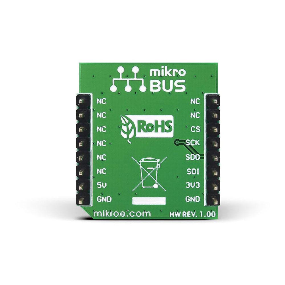
This table shows how the pinout on the EEPROM2 Click Board™ corresponds to the pinout on the mikroBUS™ socket (the latter shown in the two middle columns).
Notes | Pin | Pin | Notes | ||||
---|---|---|---|---|---|---|---|
NC | 1 | AN | PWM | 16 | NC | ||
NC | 2 | RST | INT | 15 | NC | ||
Chip Select | CS | 3 | CS | RX | 14 | NC | |
SPI Clock | SCK | 4 | SCK | TX | 13 | NC | |
SPI Data OUT | SDO | 5 | MISO | SCL | 12 | NC | |
SPI Data IN | SDI | 6 | MOSI | SDA | 11 | NC | |
Power Supply | +3V3 | 7 | 3.3V | 5V | 10 | +5V | Power Supply |
Ground | GND | 8 | GND | GND | 9 | GND | Ground |
ONBOARD SETTINGS AND INDICATORS
Label | Name | Default | Description |
---|---|---|---|
JP1 | PWR.SEL. | Left | Logic voltage level selection: left position 3V3, right position 5V |
LD1 | PWR | Power indication LED |
Software Support
We provide a library for the EEPROM2 Click Board™ on our Libstock page, as well as a demo application (example), developed using MikroElektronika compilers and mikroSDK. The provided click library is mikroSDK standard compliant. The demo application can run on all the main MikroElektronika development boards.
Library Description
This library provides generic functions enough to have complete control over the EEPROM2 Click Board™.
Key functions:
void eeprom2_writeBytes(uint32_t memoryAddress, uint8_t *value, uint8_t count)
- Writes the function to EEPROM.void eeprom2_readBytes(uint32_t memoryAddress, uint8_t *value, uint8_t count)
- Reads the function from EEPROM.void eeprom2_memoryEnable()
- Enables the write function.
Example Description
The application is composed of three sections:
- System Initialization - CS GPIO as the output pin, initializes SPI and UART for logging.
- Application Initialization - Initializes EEPROM 2 driver.
- Application Task - writing data to EEPROM, reading that data and displaying it via UART.
void applicationTask() { eeprom2_memoryEnable(); eeprom2_writeBytes(0x01, &text[0], 6); mikrobus_logWrite("Writing Mikroe to EEPROM 2 click", _LOG_LINE); Delay_ms(1000); eeprom2_readBytes(0x01,&memValue[0],6); mikrobus_logWrite("Data read:", _LOG_LINE); mikrobus_logWrite(memValue, _LOG_LINE); Delay_ms(1000); }
The full application code, and ready to use projects can be found on our Libstock page.
Other mikroE Libraries used in the example:
- I2C
- UART
Additional Notes and Information
Depending on the development board you are using, you may need a USB UART click, USB UART 2 click or RS232 click to connect to your PC, for development systems with no UART to USB interface available on the board. The terminal available in all MikroElektronika compilers, or any other terminal application of your choice, can be used to read the message.
MIKROSDK
The EEPROM2 Click Board™ is supported by mikroSDK - MikroElektronika Software Development Kit. To ensure proper operation of mikroSDK compliant click board demo applications, mikroSDK should be downloaded from the LibStock and installed for the compiler you are using.
Software Support
We provide a library for the EEPROM2 Click Board™ on our Libstock page, as well as a demo application (example), developed using MikroElektronika compilers and mikroSDK. The provided click library is mikroSDK standard compliant. The demo application can run on all the main MikroElektronika development boards.
Library Description
This library provides generic functions enough to have complete control over the EEPROM2 Click Board™.
Key Functions
void eeprom2_writeBytes(uint32_t memoryAddress, uint8_t *value, uint8_t count)
- Writes the function to EEPROM.void eeprom2_readBytes(uint32_t memoryAddress, uint8_t *value, uint8_t count)
- Reads the function from EEPROM.void eeprom2_memoryEnable()
- Enables the write function.
Example Description
The application is composed of three sections:
- System Initialization - CS GPIO as the output pin, initializes SPI and UART for logging.
- Application Initialization - Initializes EEPROM 2 driver.
- Application Task - writing data to EEPROM, reading that data and displaying it via UART.
void applicationTask() { eeprom2_memoryEnable(); eeprom2_writeBytes(0x01, &text[0], 6); mikrobus_logWrite("Writing Mikroe to EEPROM 2 click", _LOG_LINE); Delay_ms(1000); eeprom2_readBytes(0x01,&memValue[0],6); mikrobus_logWrite("Data read:", _LOG_LINE); mikrobus_logWrite(memValue, _LOG_LINE); Delay_ms(1000); }
The full application code, and ready to use projects can be found on our Libstock page.
Other mikroE Libraries used in the example:
- I2C
- UART
Additional Notes and Information
Depending on the development board you are using, you may need a USB UART click, USB UART 2 click or RS232 click to connect to your PC, for development systems with no UART to USB interface available on the board. The terminal available in all MikroElektronika compilers, or any other terminal application of your choice, can be used to read the message.
MIKROSDK
The EEPROM2 Click Board™ is supported by mikroSDK - MikroElektronika Software Development Kit. To ensure proper operation of mikroSDK compliant click board demo applications, mikroSDK should be downloaded from the LibStock and installed for the compiler you are using.
EEPROM 2 Click-Platine
Frequently Asked Questions
Have a Question?
Be the first to ask a question about this.