


Mikroelektronika d.o.o.
SKU: MIKROE-4126VCP Monitor 2 Click Board
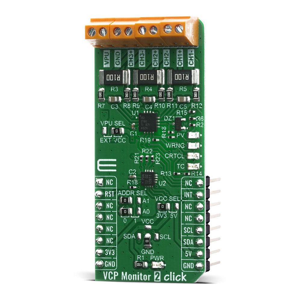
VCP Monitor 2 Click Board
Couldn't load pickup availability
The VCP Monitor 2 Click Board™ is a three-channel, high-side current and bus voltage monitor with an alert indication function ensuring the intended application works within desired operating conditions. Featured chip INA3221-Q1, by Texas Instruments, monitors both shunt voltage drops and bus supply voltages, in addition to having programmable conversion times and averaging modes for these signals. The INA3221-Q1 offers both critical and warning alerts to detect multiple programmable out-of-range conditions for each channel. The INA3221-Q1 senses current on buses that can vary from 0V to 26V.
The device is powered from a single 2.7V to 5.5V supply and draws 350 μA (typical) of supply current. The I2C and SMBUS-compatible interface features four programmable addresses.


How Does The VCP Monitor 2 Click Board™ Work?
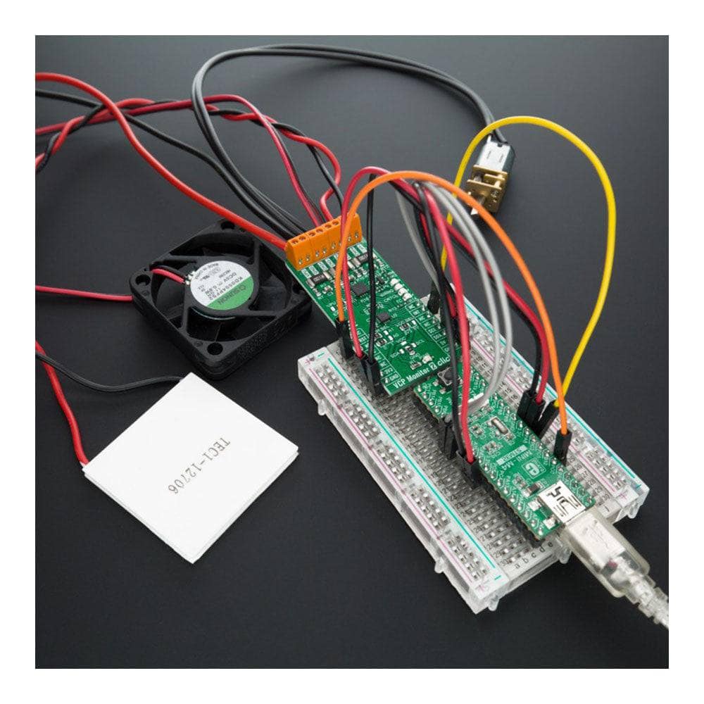
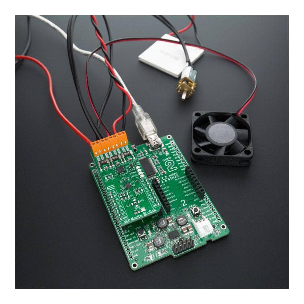
The VCP Monitor 2 Click Board™ performs two measurements on up to three power supplies of interest (CH3 - CH1). The voltage developed from the load current passing through a shunt resistor creates a shunt voltage that is measured between the IN+ and IN- pins. The device also internally measures the power supply bus voltage at the IN- pin for each channel. The differential shunt voltage is measured with respect to the IN- pin, and the bus voltage is measured with respect to ground. The featured chip which is used for channel measurements, INA3221-Q1, is typically powered by a separate power supply that ranges from 2.7V to 5.5V. The monitored supply buses range from 0V to 26V.
The INA3221-Q1 takes two measurements for each channel: one for shunt voltage and one for the bus voltage. Each measurement can be independently or sequentially measured, based on the Configuration mode settings. When the INA3221-Q1 is in the normal operating mode the device continuously converts a shunt-voltage reading followed by a bus-voltage reading. This procedure converts one channel, and then continues to the shunt voltage reading of the next enabled channel, followed by the bus-voltage reading for that channel, and so on, until all enabled channels have been measured. The programmed Configuration register mode setting applies to all channels. Any channels that are not enabled are bypassed in the measurement sequence, regardless of mode setting.
The INA3221-Q1 has two operating modes, continuous and single-shot, that determine the internal ADC operation after these conversions complete. When the INA3221-Q1 is set to continuous mode, the device continues to cycle through all enabled channels until a new configuration setting is programmed. The Configuration register MODE control bits also enable modes to be selected that convert only the shunt or bus voltage. This feature further allows the device to fit specific application requirements. In single-shot (triggered) mode, setting any single-shot convert mode to the Configuration register triggers a single-shot conversion. This action produces a single set of measurements for all enabled channels. To trigger another single-shot conversion, write to the Configuration register a second time, even if the mode does not change. When a single-shot conversion is initiated, all enabled channels are measured once, and then the device enters a power-down state. The INA3221-Q1 registers can be read at any time, even while in power-down. In addition to the two operating modes, the INA3221-Q1 also has a separate selectable power-down mode that reduces the quiescent current and turns off current into the INA3221-Q1 inputs. Power-down mode reduces the impact of the supply drain when the device is not used. Full recovery from power-down mode requires 40 µs. The INA3221-Q1 registers can be written to and read from while the device is in power-down mode. The device remains in power-down mode until one of the active MODE settings are written to the Configuration register.
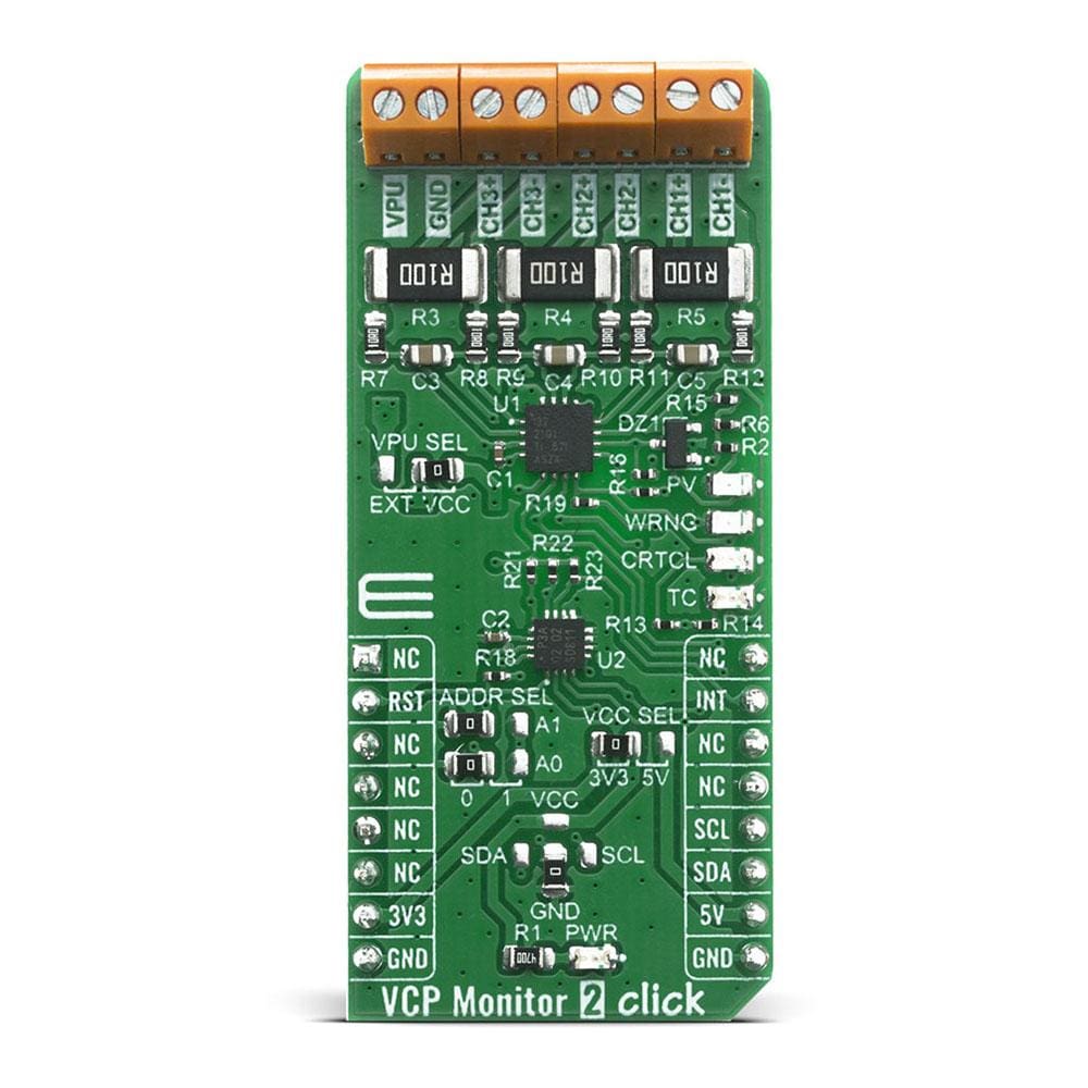
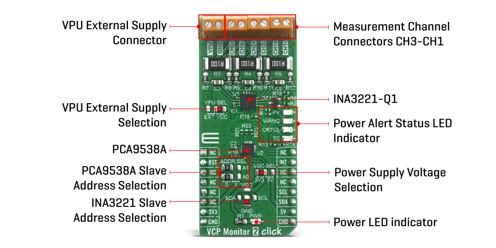
The VCP Monitor 2 Click Board™ also provides programmable thresholds that make sure the intended application operates within the desired operating conditions. Multiple monitoring functions are available using four alert pins: Critical, Warning, PV (power valid), and TC (timing control). The status of these alert pins are accessible over PCA9538A, a low-voltage 8-bit GPIO expander with interrupt and reset. The open-drain interrupt (INT) output is activated when any of the alert pins state has changed. This signal is used to inform the microcontroller that the bus voltage is not within the desired operating conditions. The PCA9538A uses the I2C communication protocol to read the current states of the alert monitoring pins with the changeable slave address to avoid bus conflict in advanced systems. For the visual representation of any deviation from programmed thresholds, alert monitoring pins are connected to 4 LEDs located on Click board™.
The VCP Monitor 2 Click Board™k supports the I2C communication protocol. Since there are two slave devices on the Click board™, the solderable SMD jumpers are conveniently placed for easy I2C slave address reconfiguration. The INA3221-Q1 has one cross-shaped jumper selection for one address pin with four possible addresses with connections to GND, VCC, SDA or SCL. The other one, PCA9538A, has two jumpers for address pins A1 and A0 with the possibility of four different slave addresses, making this Click board™ flexible for implementation in other systems with various peripherals sharing the same bus.
I2C SLAVE ADDRESS SELECTION
| A1 | A0 | PCA9538A |
|---|---|---|
| GND | GND | 0x70 |
| GND | VCC | 0x71 |
| VCC | GND | 0x72 |
| VCC | VCC | 0x73 |
| A0 | INA3221-Q1 |
|---|---|
| GND | 0x40 |
| VCC | 0x41 |
| SDA | 0x42 |
| SCL | 0x43 |
The VCP Monitor 2 Click Board™ can be supplied and interfaced with both 3.3V and 5V without needing external components. The onboard SMD jumper labelled VCC SEL allows voltage selection for interfacing with both 3.3V and 5V microcontrollers.
SPECIFICATIONS
| Type | Measurements |
| Applications | Electronic control units, digital clusters, rear-seat entertainment, infotainment, computers, power management, telecom equipment, battery chargers, power supplies, test equipment. |
| On-board modules | VCP Monitor 2 Click uses the INA3221-Q1, a three-channel, high-side current and bus voltage monitor, from Texas Instruments and PCA9538A, an IO expander with interrupt and reset, from NXP Semiconductors. |
| Key Features | Shunt voltage drops and bus supply voltages monitoring, programmable conversion times, critical and warning alerts, single power supply, 350 μA of supply current |
| Interface | I2C |
| Compatibility | mikroBUS |
| Click board size | L (57.15 x 25.4 mm) |
| Input Voltage | 3.3V or 5V |
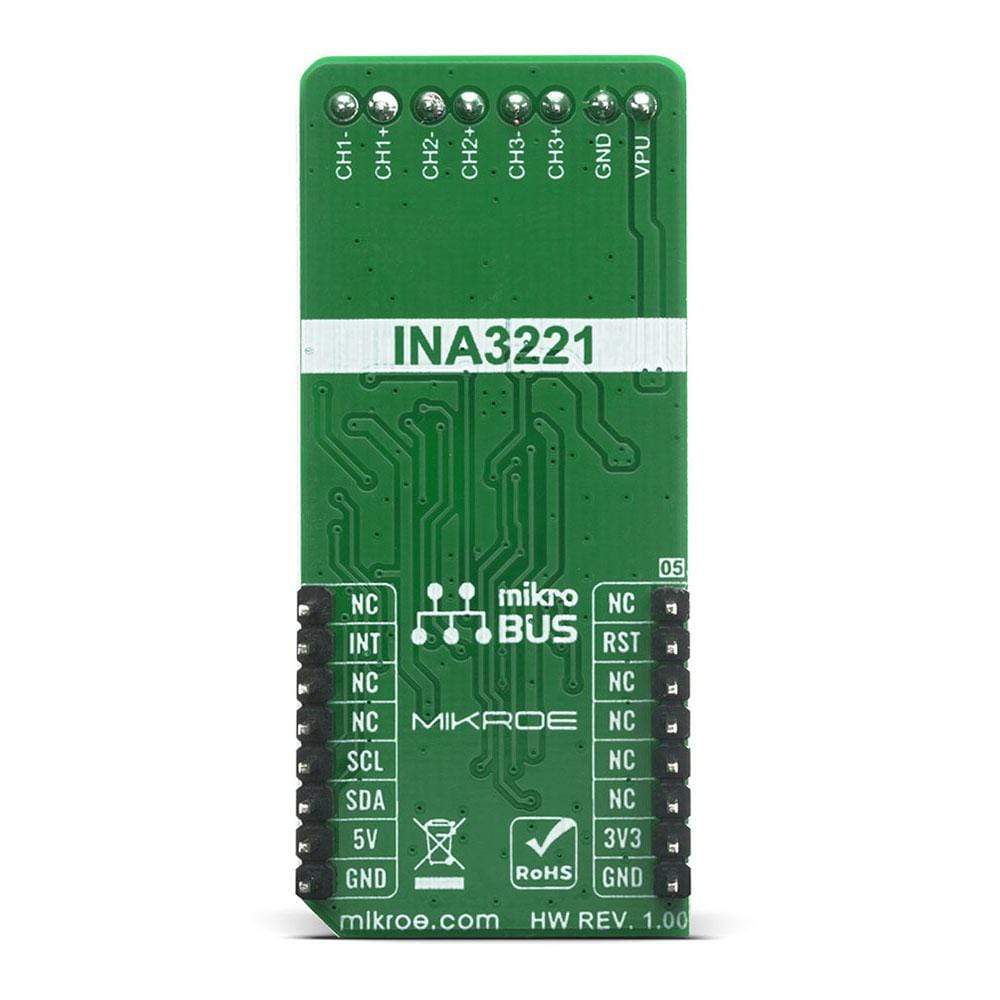
PINOUT DIAGRAM
This table shows how the VCP Monitor 2 Click Board™ pinout corresponds to the pinout on the mikroBUS™ socket (the latter shown in the two middle columns).
| Notes | Pin | Pin | Notes | ||||
|---|---|---|---|---|---|---|---|
| NC | 1 | AN | PWM | 16 | NC | ||
| NC | 2 | RST | INT | 15 | INT | Interrupt | |
| Reset | RST | 3 | CS | RX | 14 | NC | |
| NC | 4 | SCK | TX | 13 | NC | ||
| NC | 5 | MISO | SCL | 12 | SCL | I2C Clock | |
| NC | 6 | MOSI | SDA | 11 | SDA | I2C Data | |
| Power Supply | 3.3V | 7 | 3.3V | 5V | 10 | 5V | Power Supply |
| Ground | GND | 8 | GND | GND | 9 | GND | Ground |
ONBOARD SETTINGS AND INDICATORS
| Label | Name | Default | Description |
|---|---|---|---|
| LD1 | PWR | - | Power LED Indicator |
| LD2 | PV | - | Power Valid Alert LED Indicator |
| LD3 | WRNG | - | Warning Alert LED Indicator |
| LD4 | CRTCL | - | Critical Alert LED Indicator |
| LD5 | TC | - | Timing-Control Alert LED Indicator |
| JP1 | VCC SEL | Left | Power Supply Voltage Selection 3V3/5V, left position 3v3, right position 5v |
| JP2 | VPU SEL | Right | INA3221-Q1 bias supply voltage for power valid output circuitry: left position - External supply, right position - On-board supply |
| JP3, JP5 | ADDR SEL | Left | PCA9538A slave address selection: left position 0, right position 1 |
| JP4,JP6 | ADDR SEL | Down | INA3221-Q1 slave address 4-position selection: down - GND, up - VCC, left - SDA, right - SCL |
VCP MONITOR 2 CLICK ELECTRICAL SPECIFICATIONS
| Description | Min | Typ | Max | Unit |
|---|---|---|---|---|
| Supply Voltage (VCC) | 0 | 3.3 | 6 | V |
| Analog Inputs (IN+,IN-) | -0.3 | - | 26 | V |
| Bus Power Supply Rail (VPU) | 0 | - | 26 | V |
| Operating Temperature Range | -40 | - | 125 | °C |
Software Support
We provide a library for the VCP Monitor 2 Click Board™ on our LibStock page and a demo application (example), developed using MikroElektronika compilers. The demo can run on all the main MikroElektronika development boards.
Library Description
The library contains essential communication with the module and allows the user to read and write data to the module. The user can read the current data of current, voltage and power measured by the sensor.
Key Functions
float vcpmonitor2_get_shunt_voltage ( uint8_t channel )- Get Shunt voltage in mVfloat vcpmonitor2_get_current ( uint8_t channel )- Get Current data in mAfloat vcpmonitor2_get_power ( uint8_t channel )- Get Power in W
Example Description
The application is composed of three sections :
- System Initialization - Initialization I2C module and RST pin on OUTPUT
- Application Initialization - Initiaization driver init, device configuration for measurement, alert status reset and configuration
- Application Task - Display Voltage on the BUS and Shunt, current and power data. Display Alert status information.
void application_task ( )
{
 mikrobus_logWrite( ">> CHANNEL 1 <<", _LOG_LINE );
 display_channel_data( VCPMONITOR2_CHANNEL_1 );
 mikrobus_logWrite( ">> CHANNEL 2 <<", _LOG_LINE );
 display_channel_data( VCPMONITOR2_CHANNEL_2 );
 mikrobus_logWrite( ">> CHANNEL 3 <<", _LOG_LINE );
 display_channel_data( VCPMONITOR2_CHANNEL_3 );
 display_alert_status( );
 mikrobus_logWrite( "---------------------", _LOG_LINE );
 Delay_ms( 4000 );
}
Additional Functions :
- display_alert_status() - Alert status
- display_channel_data() - Channel data
The complete application code, and ready to use projects can be found on our LibStock page.
Other mikroE Libraries used in the example:
- I2C Library
- UART Library
Additional Notes and Information
Depending on the development board you are using, you may need USB UART Click Board™, USB UART 2 Click Board™ or RS232 Click Board™ to connect to your PC, for development systems with no UART to USB interface available on the board. The terminal available in all MikroElektronika compilers, or any other terminal application of your choice, can be used to read the message.
MIKROSDK
The VCP Monitor 2 Click Board™ is supported with mikroSDK - MikroElektronika Software Development Kit. To ensure proper operation of mikroSDK compliant Click board™ demo applications, mikroSDK should be downloaded from the LibStock and installed for the compiler you are using.
VCP Monitor 2 Click Board
Frequently Asked Questions
Have a Question?
Be the first to ask a question about this.