# Title: nvSRAM Click Board™
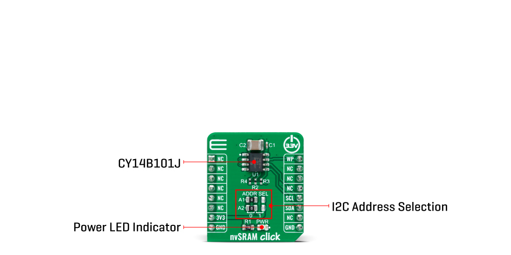
## Description: How Does The nvSRAM Click Board™ Work? The nvSRAM Click Board™ is based on the CY14B101J, a 1-Mbit nvSRAM organized as 128K words of 8 bits each with a nonvolatile element in each memory cell from Cypress Semiconductor. The CY14B101J integrates an SRAM cell and a nonvolatile memory cell into a single nvSRAM cell. In the Normal mode, all reads and writes happen directly from and to the SRAM portion of the nvSRAM. This provides faster write and read access compared to any existing nonvolatile memory technology such as EEPROM and Flash. The nvSRAM specifies one million endurance cycles for nonvolatile cells with data retention of a minimum of 20 years. In the event of system power loss, data from the SRAM is transferred to its nonvolatile cell automatically by using energy stored in a capacitor labeled as C2. During the Power-Up, data from the nonvolatile cell is recalled automatically in the SRAM array and available to the user. The endurance cycle is consumed only when data transfer happens from the SRAM cells to nonvolatile cells during the Power-Down. nvSRAM Click communicates with MCU using the standard I2C 2-Wire interface with a clock frequency up to 100kHz in the Standard, up to 400kHz in the Fast, up to 1MHz in the FastPlus, and up to 3.4MHz in the High-Speed Mode. The CY14B101J offers zero cycle delay write operation with infinite SRAM write endurance. Besides, it also allows the choice of the least significant bit (LSB) of its I2C slave address by positioning SMD jumpers labeled as ADDR SEL to an appropriate position marked as 0 and 1. An additional feature of this Click board™ represents the configurable Write Protection function labeled as WP routed on the PWM pin of the mikroBUS™ socket. The WP pin is an active-high pin that protects the entire memory and all registers from write operations. This pin must be held high to inhibit all the write operations. When this pin is high, all memory and register writes are prohibited, and the address counter is not incremented. This Click board™ is designed to be operated only with a 3.3V logic voltage level. A proper logic voltage level conversion should be performed before the Click board™ is used with MCUs with different logic levels. SPECIFICATIONS Type SRAM Applications Can be used for all applications that require fast access and high reliability of stored data, and unlimited endurance. On-board modules nvSRAM Click is based on the CY14B101J, a 1-Mbit nvSRAM organized as 128K words of 8 bits each with a nonvolatile element in each memory cell from Cypress Semiconductor. Key Features Low power consumption, 1-Mbit nonvolatile static random access memory, high reliability, high speed interface, write protection feature, and more. Interface I2C Compatibility mikroBUS Click board size S (28.6 x 25.4 mm) Input Voltage 3.3V PINOUT DIAGRAM This table shows how the pinout on nvSRAM Click corresponds to the pinout on the mikroBUS™ socket (the latter shown in the two middle columns). Notes Pin Pin Notes NC 1 AN PWM 16 WP Write Protection NC 2 RST INT 15 NC NC 3 CS RX 14 NC NC 4 SCK TX 13 NC NC 5 MISO SCL 12 SCL I2C Clock NC 6 MOSI SDA 11 SDA I2C Data Power Supply 3.3V 7 3.3V 5V 10 NC Ground GND 8 GND GND 9 GND Ground ONBOARD SETTINGS AND INDICATORS Label Name Default Description LD1 PWR - Power LED Indicator JP1-JP2 ADDR SEL Left I2C Address Selection: Left position 0, Right position 1 NVSRAM CLICK ELECTRICAL SPECIFICATIONS Description Min Typ Max Unit Supply Voltage -0.5 3.3 4.1 V Memory Size - - 1 Mbit nvSRAM Write Endurance 1.000.000 - - Write Cycles nvSRAM Data Retention 20 - - Years Operating Temperature Range -40 - +85 °C
## Product type: Click Board
## Vendor: Mikroelektronika d.o.o.
## Tags: Click Board, Cypress, Memory, MikroE, SRAM
## Price range: 25.2 - 25.2 GBP
## Link: https://thedebugstore.com/products/mikroe-4441-nvsram-click-board-uk
## Compare-at price range: 36.0 - 36.0 GBP
## Options
- Title: Default Title
## Collections
- [New Products](https://thedebugstore.com/a/llms/collections/new-products-debug-store)
- [Mikroelektronika d.o.o. (MikroE)](https://thedebugstore.com/a/llms/collections/mikroelektronika-catalogue-uk)
- [Cypress PSoC Development Boards & Tools | Debug Store](https://thedebugstore.com/a/llms/collections/cypress-device-support)
- [Memory Device Click Boards™](https://thedebugstore.com/a/llms/collections/memory-device-click-boards-catalogue-uk)
- [MikroE Click Boards™](https://thedebugstore.com/a/llms/collections/mikroe-click-boards-catalogue-uk)
- [SRAM Click Boards™](https://thedebugstore.com/a/llms/collections/sram-click-boards-catalogue)
- [Click Boards™ Summer Sale](https://thedebugstore.com/a/llms/collections/inventory-sale)
- [MikroE Sale](https://thedebugstore.com/a/llms/collections/mikroe-sale)
- [MIKROE Stock](https://thedebugstore.com/a/llms/collections/mikroe-products-in-stock-sale)
## Variants
- Default Title, SKU: MIKROE-4441, Available: yes, Inventory: 1
## Metafields
- full_description: How Does The nvSRAM Click Board™ Work?
The nvSRAM Click Board™ is based on the CY14B101J, a 1-Mbit nvSRAM organized as 128K words of 8 bits each with a nonvolatile element in each memory cell from Cypress Semiconductor. The CY14B101J integrates an SRAM cell and a nonvolatile memory cell into a single nvSRAM cell. In the Normal mode, all reads and writes happen directly from and to the SRAM portion of the nvSRAM. This provides faster write and read access compared to any existing nonvolatile memory technology such as EEPROM and Flash.
The nvSRAM specifies one million endurance cycles for nonvolatile cells with data retention of a minimum of 20 years. In the event of system power loss, data from the SRAM is transferred to its nonvolatile cell automatically by using energy stored in a capacitor labeled as C2. During the Power-Up, data from the nonvolatile cell is recalled automatically in the SRAM array and available to the user. The endurance cycle is consumed only when data transfer happens from the SRAM cells to nonvolatile cells during the Power-Down.
nvSRAM Click communicates with MCU using the standard I2C 2-Wire interface with a clock frequency up to 100kHz in the Standard, up to 400kHz in the Fast, up to 1MHz in the FastPlus, and up to 3.4MHz in the High-Speed Mode. The CY14B101J offers zero cycle delay write operation with infinite SRAM write endurance. Besides, it also allows the choice of the least significant bit (LSB) of its I2C slave address by positioning SMD jumpers labeled as ADDR SEL to an appropriate position marked as 0 and 1.
An additional feature of this Click board™ represents the configurable Write Protection function labeled as WP routed on the PWM pin of the mikroBUS™ socket. The WP pin is an active-high pin that protects the entire memory and all registers from write operations. This pin must be held high to inhibit all the write operations. When this pin is high, all memory and register writes are prohibited, and the address counter is not incremented.
This Click board™ is designed to be operated only with a 3.3V logic voltage level. A proper logic voltage level conversion should be performed before the Click board™ is used with MCUs with different logic levels.
SPECIFICATIONS
| Type |
SRAM |
| Applications |
Can be used for all applications that require fast access and high reliability of stored data, and unlimited endurance. |
| On-board modules |
nvSRAM Click is based on the CY14B101J, a 1-Mbit nvSRAM organized as 128K words of 8 bits each with a nonvolatile element in each memory cell from Cypress Semiconductor. |
| Key Features |
Low power consumption, 1-Mbit nonvolatile static random access memory, high reliability, high speed interface, write protection feature, and more. |
| Interface |
I2C |
| Compatibility |
mikroBUS |
| Click board size |
S (28.6 x 25.4 mm) |
| Input Voltage |
3.3V |
PINOUT DIAGRAM
This table shows how the pinout on nvSRAM Click corresponds to the pinout on the mikroBUS™ socket (the latter shown in the two middle columns).
| Notes |
Pin |
 |
Pin |
Notes |
| NC |
1 |
AN |
PWM |
16 |
WP |
Write Protection |
| NC |
2 |
RST |
INT |
15 |
NC |
| NC |
3 |
CS |
RX |
14 |
NC |
| NC |
4 |
SCK |
TX |
13 |
NC |
| NC |
5 |
MISO |
SCL |
12 |
SCL |
I2C Clock |
| NC |
6 |
MOSI |
SDA |
11 |
SDA |
I2C Data |
| Power Supply |
3.3V |
7 |
3.3V |
5V |
10 |
NC |
| Ground |
GND |
8 |
GND |
GND |
9 |
GND |
Ground |
ONBOARD SETTINGS AND INDICATORS
| Label |
Name |
Default |
Description |
| LD1 |
PWR |
- |
Power LED Indicator |
| JP1-JP2 |
ADDR SEL |
Left |
I2C Address Selection: Left position 0, Right position 1 |
NVSRAM CLICK ELECTRICAL SPECIFICATIONS
| Description |
Min |
Typ |
Max |
Unit |
| Supply Voltage |
-0.5 |
3.3 |
4.1 |
V |
| Memory Size |
- |
- |
1 |
Mbit |
| nvSRAM Write Endurance |
1.000.000 |
- |
- |
Write Cycles |
| nvSRAM Data Retention |
20 |
- |
- |
Years |
| Operating Temperature Range |
-40 |
- |
+85 |
°C |
- description_tag: The nvSRAM Click Board™ is a compact add-on board that contains the most reliable nonvolatile memory. This board features the CY14B101J, a 1-Mbit nvSRAM organized as 128K words of 8 bits each with a nonvolatile element in each memory cell from Cypress Semiconductor. Available from Debug Store UK.
- title_tag: MikroE nvSRAM Click Board™ (MIKROE-4441)
- manufacturer: Mikroelektronika d.o.o.
- warranty: 12 months
- amazon_enable: TRUE
- amazon_title: SRAM Click Board
- amazon_product_type: computercomponent
- amazon_block: FALSE
- amazon_prime_enable: FALSE
- amazon_search: MikroElektronika Microelectronica MIKROE-1100
- amazon_uk_price: 13.2
- amazon_uk_currency: GBP
- amazon_de_currency: EUR
- amazon_de_price: 14.916
- amazon_fr_currency: EUR
- amazon_fr_price: 14.916
- amazon_es_currency: EUR
- amazon_es_price: 14.916
- amazon_nl_currency: EUR
- amazon_nl_price: 14.916
- amazon_it_currency: EUR
- amazon_it_price: 14.916
- amazon_se_curency: SEK
- amazon_se_price: 150.48
- amazon_product_id: 8606015076683
- amazon_product_id_type: EAN
- amazon_update: Update
- amazon_short_description: The MikroE SRAM Click Board™ is a storage add-on board that carries the 23LC1024 IC, which allows the user to add 1Mbit of additional SRAM (static RAM) memory to the device. Based on low-power CMOS technology, the 23LC1024 chip outlines the memory in 8-bit instruction registers and 32-byte pages (128K x 8-bit). For Read and Write operations, this highly-reliable chip offers byte, page, and sequential operating modes. The sequential mode enables Read/Write operation for an entire memory array.It supports unlimited Read/Write cycles to the memory array with zero Write time. It operates at a clock rate of 20 MHz for all the three Read/Write modes. Communicating through SPI-Compatible bus interface, the board also has an additional Hold pin functionality in place of the default RST pin. SRAM Click Board™ can be used with either 3.3V or 5V power supply.
- amazon_long_description: IC/Module: 23LC1024
23LC1024 IC allows user to add 1 Mbit (megabit) of extra storage to your design and carry out infinite Read and Write operations to the memory array. This highly reliable and low power chip allows memory access via a simple SPI-compatible serial bus. However, it is compatible with SPI (Serial Peripheral Interface), SDI (Serial Dual Interface) and SQI (Serial Quad Interface).
.
1Mbit Storage
The 1 Mbit of additional storage provided by the 23LC1024 IC is divided into the form of 8-bit instruction registers and 32-byte write pages.
SPI Interface (20 MHz clock rate)
SRAM Click communicates with the target microcontroller through the mikroBUS SPI interface using the MISO, MOSI, SCK, CS pins. It has an additional HOLD functionality provided through the default mikroBUS RST pin. When the HLD pin is pulled low, it causes suspension of the data transmission mid-sequence rather than causing the reset of the whole sequence.
- amazon_main_image: https://www.thedebugstore.com/images/product/lg-mikroe-click-sram_1_1.jpg
- amazon_browse_node: 428655031
- mpn: MIKROE-4441
- backorder_label: If no stock shown above, check availability
- attachment_url_1: https://www.thedebugstore.com/files/attachments/14437/nvSRAM-click-schematic-v100.pdf&&https://www.thedebugstore.com/files/attachments/14437/CY14B101J_datasheet.pdf
- attachment_title_1: nvSRAM Click Board™ Schematic&&Cypress CY14B101J nvSRAM Datasheet
- google_product_category: 288
- examples:
We provide a library for the nvSRAM Click Board™ on our LibStock page, as well as a demo application (example), developed using MikroElektronika compilers. The demo can run on all the main MikroElektronika development boards.
Library Description
The library covers all the necessary functions to control nvSRAM Click board™. Library performs a standard I2C interface communication.
Key Functions
uint32_t nvsram_read_dev_id ( void ) - Read device ID function.void nvsram_memory_write ( uint32_t mem_adr, uint8_t *p_tx_data, uint16_t n_bytes ) - Write memory function.void nvsram_memory_read ( uint32_t mem_adr, uint8_t *p_rx_data, uint16_t n_bytes ) - Read memory function.
Example Description
The application is composed of three sections :
- System Initialization - Initializes I2C, set PWM pin as outputs, begins to write log.
- Application Initialization - Initialization driver enables - I2C, lock Serial Number write, disable Block Protection and enable Memory Write, also write log.
- Application Task - (code snippet) This is an example that demonstrates the use of the nvSRAM Click board™. In this example, we write and then read data from nvSRAM memory. Results are being sent to the Usart Terminal where you can track their changes. All data logs write on USB uart changes approximately for every 5 sec.
{
 mikrobus_logWrite( " Write data : ", _LOG_TEXT );
 mikrobus_logWrite( demo_data, _LOG_TEXT );
 nvsram_memory_write( 12345, &demo_data[ 0 ], 9 );
 mikrobus_logWrite( "- - - - - - - - - - - -", _LOG_LINE );
 Delay_ms( 100 );
 mikrobus_logWrite( " Read data : ", _LOG_TEXT );
 nvsram_memory_read( 12345, &read_data[ 0 ], 9 );
 mikrobus_logWrite( read_data, _LOG_TEXT );
 mikrobus_logWrite( "-----------------------", _LOG_LINE );
 Delay_ms( 5000 );
}
The full application code, and ready to use projects can be found on our LibStock page.
Other mikroE Libraries used in the example:
Additional Notes and Information
Depending on the development board you are using, you may need USB UART click, USB UART 2 click or RS232 click to connect to your PC, for development systems with no UART to USB interface available on the board. The terminal available in all MikroElektronika compilers, or any other terminal application of your choice, can be used to read the message.
MIKROSDK
This Click board™ is supported with mikroSDK - MikroElektronika Software Development Kit. To ensure proper operation of mikroSDK compliant Click board™ demo applications, mikroSDK should be downloaded from the LibStock and installed for the compiler you are using.
- attachments: [{"download_file":[{"download_file":"nvSRAM Click Board™ Schematic"}],"download_filetype":[{"download_filetype":"pdf"}]},{"download_file":[{"download_file":"Cypress CY14B101J 1Mbit nvSRAM Datasheet"}],"download_filetype":[{"download_filetype":"pdf"}]}]
- condition: new
- custom_product: false
- mpn: MIKROE-4441
- google_product_category: Electronics
- custom_label_0: Click Board
- device_vendor: Cypress Semiconductor Corp
- device_type: CY14B101J2-SXI
- warranty: 12 months
- brand: MikroE
- key_feature_1: 1Mb I2C nvSRAM
- manufacturer: Mikroelektronika d.o.o.
- badge: No reviews
- widget:
- target_keyword: nvSRAM Click Board
- brands: gid://shopify/Metaobject/56256004319
- breadcrumbs: ["gid://shopify/Collection/447955239135","gid://shopify/Collection/241680580797","gid://shopify/Collection/241545183421"]
- customhs_code: 847330
- detailed_description: {"type":"root","children":[{"type":"heading","level":3,"children":[{"type":"text","value":"How Does The nvSRAM Click Board™ Work?"}]},{"type":"paragraph","children":[{"type":"text","value":"The "},{"type":"text","value":"nvSRAM Click Board™","bold":true,"italic":true},{"type":"text","value":" is based on the CY14B101J, a 1-Mbit nvSRAM organized as 128K words of 8 bits each with a nonvolatile element in each memory cell from Cypress Semiconductor. The CY14B101J integrates an SRAM cell and a nonvolatile memory cell into a single nvSRAM cell. In the Normal mode, all reads and writes happen directly from and to the SRAM portion of the nvSRAM. This provides faster write and read access compared to any existing nonvolatile memory technology such as EEPROM and Flash."}]},{"type":"paragraph","children":[{"type":"text","value":""}]},{"type":"paragraph","children":[{"type":"text","value":"The nvSRAM specifies one million endurance cycles for nonvolatile cells with data retention of a minimum of 20 years. In the event of system power loss, data from the SRAM is transferred to its nonvolatile cell automatically by using energy stored in a capacitor labeled as C2. During the Power-Up, data from the nonvolatile cell is recalled automatically in the SRAM array and available to the user. The endurance cycle is consumed only when data transfer happens from the SRAM cells to nonvolatile cells during the Power-Down."}]},{"type":"paragraph","children":[{"type":"text","value":"nvSRAM Click communicates with MCU using the standard I2C 2-Wire interface with a clock frequency up to 100kHz in the Standard, up to 400kHz in the Fast, up to 1MHz in the FastPlus, and up to 3.4MHz in the High-Speed Mode. The CY14B101J offers zero cycle delay write operation with infinite SRAM write endurance. Besides, it also allows the choice of the least significant bit (LSB) of its I2C slave address by positioning SMD jumpers labeled as ADDR SEL to an appropriate position marked as 0 and 1."}]},{"type":"paragraph","children":[{"type":"text","value":"An additional feature of this Click board™ represents the configurable Write Protection function labeled as WP routed on the PWM pin of the mikroBUS™ socket. The WP pin is an active-high pin that protects the entire memory and all registers from write operations. This pin must be held high to inhibit all the write operations. When this pin is high, all memory and register writes are prohibited, and the address counter is not incremented."}]},{"type":"paragraph","children":[{"type":"text","value":"This Click board™ is designed to be operated only with a 3.3V logic voltage level. A proper logic voltage level conversion should be performed before the Click board™ is used with MCUs with different logic levels."}]},{"type":"heading","level":3,"children":[{"type":"text","value":"SPECIFICATIONS"}]},{"type":"paragraph","children":[{"type":"text","value":"Type\nSRAM\nApplications\nCan be used for all applications that require fast access and high reliability of stored data, and unlimited endurance.\nOn-board modules\nnvSRAM Click is based on the CY14B101J, a 1-Mbit nvSRAM organized as 128K words of 8 bits each with a nonvolatile element in each memory cell from Cypress Semiconductor.\nKey Features\nLow power consumption, 1-Mbit nonvolatile static random access memory, high reliability, high speed interface, write protection feature, and more.\nInterface\nI2C\nCompatibility\nmikroBUS\nClick board size\nS (28.6 x 25.4 mm)\nInput Voltage\n3.3V"}]},{"type":"heading","level":3,"children":[{"type":"text","value":"PINOUT DIAGRAM"}]},{"type":"paragraph","children":[{"type":"text","value":"This table shows how the pinout on nvSRAM Click corresponds to the pinout on the mikroBUS™ socket (the latter shown in the two middle columns)."}]},{"type":"paragraph","children":[{"type":"text","value":"Notes\nPin\nPin\nNotes\nNC\n1\nAN\nPWM\n16\nWP\nWrite Protection\nNC\n2\nRST\nINT\n15\nNC\nNC\n3\nCS\nRX\n14\nNC\nNC\n4\nSCK\nTX\n13\nNC\nNC\n5\nMISO\nSCL\n12\nSCL\nI2C Clock\nNC\n6\nMOSI\nSDA\n11\nSDA\nI2C Data\nPower Supply\n3.3V\n7\n3.3V\n5V\n10\nNC\nGround\nGND\n8\nGND\nGND\n9\nGND\nGround"}]},{"type":"heading","level":3,"children":[{"type":"text","value":"ONBOARD SETTINGS AND INDICATORS"}]},{"type":"paragraph","children":[{"type":"text","value":"Label\nName\nDefault\nDescription\nLD1\nPWR\n-\nPower LED Indicator\nJP1-JP2\nADDR SEL\nLeft\nI2C Address Selection: Left position 0, Right position 1"}]},{"type":"heading","level":3,"children":[{"type":"text","value":"NVSRAM CLICK ELECTRICAL SPECIFICATIONS"}]},{"type":"paragraph","children":[{"type":"text","value":"Description\nMin\nTyp\nMax\nUnit\nSupply Voltage\n-0.5\n3.3\n4.1\nV\nMemory Size\n-\n-\n1\nMbit\nnvSRAM Write Endurance\n1.000.000\n-\n-\nWrite Cycles\nnvSRAM Data Retention\n20\n-\n-\nYears\nOperating Temperature Range\n-40\n-\n+85\n°C"}]},{"type":"heading","level":3,"children":[{"type":"text","value":" "}]}]}
- summary: The nvSRAM Click Board™ is a compact add-on board that contains the most reliable nonvolatile memory. This board features the CY14B101J, a 1-Mbit nvSRAM organized as 128K words of 8 bits each with a nonvolatile element in each memory cell from Cypress Semiconductor. The embedded nonvolatile elements incorporate the QuantumTrap technology and provide highly reliable nonvolatile storage of data. Data transfer, initiated by the user through I2C commands, from SRAM to the nonvolatile elements takes place automatically at Power-Down. On the other hand, during the Power-Up, data is restored to the SRAM from the nonvolatile memory. This Click Board™ is suitable for all applications that require fast access and high reliability of stored data, and unlimited endurance.
nvSRAM Click is supported by a mikroSDK compliant library, which includes functions that simplify software development. This Click Board™ comes as a fully tested product, ready to be used on a system equipped with the mikroBUS™ socket.