# Title: NFC 2 Click Board™
## Description: How Does The NFC 2 Click Board™ Work? The NFC 2 Click Board™ is based on the PN7150, high-performance full NFC solution with integrated firmware and I2C interface designed for contactless communication at 13.56 MHz from NXP USA Inc. This board has full compliance with NFC Forum specification that means that you will be able to use the full potential of NFC. It is the ideal solution for rapidly integrating NFC technology in any application, especially those running O/S environments like Linux and Android, reducing size and cost thanks to embedded NFC firmware providing all NFC protocols as a pre-integrated feature and ultra-low power consumption. The PN7150 embeds a microcontroller core ARM Cortex-M0 loaded with the integrated firmware and provides an easy integration and validation cycle as all the NFC real-time constraints, protocols, and device discovery are being taken care of internally. The host can configure the PN7150 to notify for a card or peer detection and start communicating with them. The core microcontroller chip of the PN7150 can run without any external clock (based on an internal oscillator). However, the 13.56MHz RF field carrier accuracy requirements are not compatible with the use of an internal oscillator. That's why the PN7150 has an external crystal oscillator connected to its XTAL pins. It also has four power states: Monitor, Hard Power Down (HPD), Standby, and Active. At the application level, the PN7150 will continuously switch between different power states to optimize the current consumption. The PN7150 is designed to allow the host controller to have full control over its operation, thus of the power consumption of the PN7150 based NFC solution and the possibility to restrict parts of the PN7150 functionality. More information about these modes user can find in the attached datasheet. The NFC 2 Click Board™ communicates with MCU using the standard I2C 2-Wire interface with a clock frequency up to 100kHz in the Standard, up to 400kHz in the Fast, and up to 3.4MHz in the High-Speed Mode. The PN7150 also allows the choice of the least significant bit (LSB) of its I2C slave address by positioning SMD jumpers labelled as ADDR SEL to an appropriate position marked as 0 and 1. To enable and ensure data flow control between PN7150 and host controller, additionally, a dedicated interrupt line labelled as INT is provided that Active state is programmable. It also contains Reset function, and the RF antenna which is used to communicate over RF with a Tag (Card) and a Reader/Writer or a Peer device. The NFC 2 Click Board™ is designed to be operated only with a 3.3V logic voltage level, while 5V is used as transmitter input supply voltage of PN7150. A proper logic voltage level conversion should be performed before the Click board™ is used with MCUs with different logic levels. However, the Click board™ comes equipped with a library that contains easy to use functions and an example code which can be used, as a reference, for further development. SPECIFICATIONS Type RFID/NFC Applications Can be used for rapidly integrating NFC technology in any application. On-board modules The NFC 2 Click Board™ is based on the PN7150, high-performance full NFC solution with integrated firmware and I2C interface designed for contactless communication at 13.56 MHz from NXP USA Inc. Key Features Ultralow power consumption, automatic wake-up via RF field, integrated non-volatile memory to store data and executable code for customization, various RF protocols supported, includes ARM Cortex-M0 microcontroller core, and more. Interface I2C Compatibility mikroBUS Click board size L (57.15 x 25.4 mm) Input Voltage 3.3V or 5V PINOUT DIAGRAM This table shows how the pinout of the NFC 2 Click Board™ corresponds to the pinout on the mikroBUS™ socket (the latter shown in the two middle columns). Notes Pin Pin Notes NC 1 AN PWM 16 NC Reset RST 2 RST INT 15 INT Interrupt NC 3 CS RX 14 NC NC 4 SCK TX 13 NC NC 5 MISO SCL 12 SCL I2C Clock NC 6 MOSI SDA 11 SDA I2C Data Power Supply 3.3V 7 3.3V 5V 10 5V Power Supply Ground GND 8 GND GND 9 GND Ground ONBOARD SETTINGS AND INDICATORS Label Name Default Description LD1 PWR - Power LED Indicator JP1-JP2 ADDR SEL Left I2C Address Selection: Left position 0, Right position 1 NFC 2 CLICK ELECTRICAL SPECIFICATIONS Description Min Typ Max Unit Supply Voltage -0.3 3.3 4.35 V Operating Frequency - 13.56 52 MHz Maximum RF Driver Current - - 180 mA Maximum Output Power - - 0.85 W Operating Temperature Range -30 +25 +85 °C
## Product type: Click Board
## Vendor: Mikroelektronika d.o.o.
## Tags: Click Board, ID, MikroE, Misc, NFC, NXP, RFid+NFC, Wireless
## Price range: 28.7 - 28.7 GBP
## Link: https://thedebugstore.com/products/mikroe-4309-nfc-2-click-board-uk
## Compare-at price range: 41.0 - 41.0 GBP
## Options
- Title: Default Title
## Collections
- [New Products](https://thedebugstore.com/a/llms/collections/new-products-debug-store)
- [Mikroelektronika d.o.o. (MikroE)](https://thedebugstore.com/a/llms/collections/mikroelektronika-catalogue-uk)
- [NXP Device Support from Debug Store: Explore Our Innovative Embedded Solutions](https://thedebugstore.com/a/llms/collections/nxp-device-support-uk)
- [Wireless Interface Click Boards™](https://thedebugstore.com/a/llms/collections/wireless-interface-click-boards-catalogue)
- [Miscellaneous Click Boards™](https://thedebugstore.com/a/llms/collections/miscellaneous-click-boards-catalogue)
- [MikroE Click Boards™](https://thedebugstore.com/a/llms/collections/mikroe-click-boards-catalogue-uk)
- [RFid/NFC Click Boards™](https://thedebugstore.com/a/llms/collections/rfid-nfc-click-boards-catalogue)
- [ID Click Boards™](https://thedebugstore.com/a/llms/collections/id-click-boards-catalogue)
- [Click Boards™ Summer Sale](https://thedebugstore.com/a/llms/collections/inventory-sale)
- [MikroE Sale](https://thedebugstore.com/a/llms/collections/mikroe-sale)
- [MIKROE Stock](https://thedebugstore.com/a/llms/collections/mikroe-products-in-stock-sale)
## Variants
- Default Title, SKU: MIKROE-4309, Available: yes, Inventory: 1
## Metafields
- full_description: How Does The NFC 2 Click Board™ Work?
The NFC 2 Click Board™ is based on the PN7150, high-performance full NFC solution with integrated firmware and I2C interface designed for contactless communication at 13.56 MHz from NXP USA Inc. This board has full compliance with NFC Forum specification that means that you will be able to use the full potential of NFC. It is the ideal solution for rapidly integrating NFC technology in any application, especially those running O/S environments like Linux and Android, reducing size and cost thanks to embedded NFC firmware providing all NFC protocols as a pre-integrated feature and ultra-low power consumption.
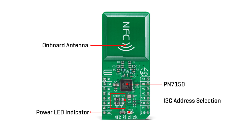
The PN7150 embeds a microcontroller core ARM Cortex-M0 loaded with the integrated firmware and provides an easy integration and validation cycle as all the NFC real-time constraints, protocols, and device discovery are being taken care of internally. The host can configure the PN7150 to notify for a card or peer detection and start communicating with them. The core microcontroller chip of the PN7150 can run without any external clock (based on an internal oscillator). However, the 13.56MHz RF field carrier accuracy requirements are not compatible with the use of an internal oscillator. That's why the PN7150 has an external crystal oscillator connected to its XTAL pins.
It also has four power states: Monitor, Hard Power Down (HPD), Standby, and Active. At the application level, the PN7150 will continuously switch between different power states to optimize the current consumption. The PN7150 is designed to allow the host controller to have full control over its operation, thus of the power consumption of the PN7150 based NFC solution and the possibility to restrict parts of the PN7150 functionality. More information about these modes user can find in the attached datasheet.
The NFC 2 Click Board™ communicates with MCU using the standard I2C 2-Wire interface with a clock frequency up to 100kHz in the Standard, up to 400kHz in the Fast, and up to 3.4MHz in the High-Speed Mode. The PN7150 also allows the choice of the least significant bit (LSB) of its I2C slave address by positioning SMD jumpers labelled as ADDR SEL to an appropriate position marked as 0 and 1. To enable and ensure data flow control between PN7150 and host controller, additionally, a dedicated interrupt line labelled as INT is provided that Active state is programmable. It also contains Reset function, and the RF antenna which is used to communicate over RF with a Tag (Card) and a Reader/Writer or a Peer device.
The NFC 2 Click Board™ is designed to be operated only with a 3.3V logic voltage level, while 5V is used as transmitter input supply voltage of PN7150. A proper logic voltage level conversion should be performed before the Click board™ is used with MCUs with different logic levels. However, the Click board™ comes equipped with a library that contains easy to use functions and an example code which can be used, as a reference, for further development.
SPECIFICATIONS
| Type |
RFID/NFC |
| Applications |
Can be used for rapidly integrating NFC technology in any application. |
| On-board modules |
The NFC 2 Click Board™ is based on the PN7150, high-performance full NFC solution with integrated firmware and I2C interface designed for contactless communication at 13.56 MHz from NXP USA Inc. |
| Key Features |
Ultralow power consumption, automatic wake-up via RF field, integrated non-volatile memory to store data and executable code for customization, various RF protocols supported, includes ARM Cortex-M0 microcontroller core, and more. |
| Interface |
I2C |
| Compatibility |
mikroBUS |
| Click board size |
L (57.15 x 25.4 mm) |
| Input Voltage |
3.3V or 5V |
PINOUT DIAGRAM
This table shows how the pinout of the NFC 2 Click Board™ corresponds to the pinout on the mikroBUS™ socket (the latter shown in the two middle columns).
| Notes |
Pin |
 |
Pin |
Notes |
| NC |
1 |
AN |
PWM |
16 |
NC |
| Reset |
RST |
2 |
RST |
INT |
15 |
INT |
Interrupt |
| NC |
3 |
CS |
RX |
14 |
NC |
| NC |
4 |
SCK |
TX |
13 |
NC |
| NC |
5 |
MISO |
SCL |
12 |
SCL |
I2C Clock |
| NC |
6 |
MOSI |
SDA |
11 |
SDA |
I2C Data |
| Power Supply |
3.3V |
7 |
3.3V |
5V |
10 |
5V |
Power Supply |
| Ground |
GND |
8 |
GND |
GND |
9 |
GND |
Ground |
ONBOARD SETTINGS AND INDICATORS
| Label |
Name |
Default |
Description |
| LD1 |
PWR |
- |
Power LED Indicator |
| JP1-JP2 |
ADDR SEL |
Left |
I2C Address Selection: Left position 0, Right position 1 |
NFC 2 CLICK ELECTRICAL SPECIFICATIONS
| Description |
Min |
Typ |
Max |
Unit |
| Supply Voltage |
-0.3 |
3.3 |
4.35 |
V |
| Operating Frequency |
- |
13.56 |
52 |
MHz |
| Maximum RF Driver Current |
- |
- |
180 |
mA |
| Maximum Output Power |
- |
- |
0.85 |
W |
| Operating Temperature Range |
-30 |
+25 |
+85 |
°C |
- description_tag: The NFC 2 Click Board™ is a compact add-on board that contains a highly integrated NFC transceiver for contactless communication. This board features the PN7150, the best plug&play high-performance full NFC solution with integrated firmware and NCI interface from NXP. Available from Debug Store UK.
- title_tag: MikroE NFC 2 Click Board™ (MIKROE-4309)
- manufacturer: Mikroelektronika d.o.o.
- warranty: 12 months
- amazon_enable: TRUE
- amazon_title: NFC Click Board
- amazon_product_type: computercomponent
- amazon_block: FALSE
- amazon_prime_enable: FALSE
- amazon_uk_price: 29.92
- amazon_uk_currency: GBP
- amazon_de_currency: EUR
- amazon_de_price: 33.8096
- amazon_fr_currency: EUR
- amazon_fr_price: 33.8096
- amazon_es_currency: EUR
- amazon_es_price: 33.8096
- amazon_nl_currency: EUR
- amazon_nl_price: 33.8096
- amazon_it_currency: EUR
- amazon_it_price: 33.8096
- amazon_se_curency: SEK
- amazon_se_price: 341.088
- amazon_product_id: 8606015079165
- amazon_product_id_type: EAN
- amazon_update: Update
- amazon_short_description: NFC Click Board™ is a mikroBUS add-on board with a versatile near field communications controller from NXP the PN7120 IC.NFC devices are used in contactless payment systems, electronic ticketing, smartcards, but also in retail and advertising inexpensive NFC tags can be embedded into packaging labels, flyers or posters.
- amazon_long_description: NFC Click is a mikroBUS add-on board with a versatile near field communications controller from NXP, the PN7120 IC. NFC devices are used in contactless payment systems, electronic ticketing, smartcards, but also in retail and advertising inexpensive NFC tags can be embedded into packaging labels, flyers or posters.
This board has full compliancy with NFC Forum specifications which means that you will be able to use the full potential of NFC and its three distinct operating modes:
1. Card emulation
2. Read/Write
3. P2P
In other words, NFC Click can be set to behave either as an NFC reader, or a tag, or to establish a two-way connection with another NFC device.
Fully Compliant and Easy to Integrate
The NXP's PN7120 IC integrates an ARM Cortex-M0 MCU, which enables easier integration into designs, because it requires fewer resources from the host MCU. The integrated firmware provides all NFC protocols for performing the contactless communication in charge of the modulation, data processing and error detection.
The board communicates with the target board MCU through the mikroBUS I2C interface, in compliance with NCI 1.0 host protocols (NCI stands for NFC controller interface). RST and INT pins provide additional functionality. The board uses a 3.3V power supply.
PB7120 Features
PN7120 embeds a new generation RF contactless front-end supporting various transmission modes according to NFCIP-1 and NFCIP-2, ISO/IEC14443, ISO/IEC 15693, ISO/IEC 18000-3, MIFARE and FeliCa specifications. It embeds an ARM Cortex-M0 microcontroller core loaded with the integrated firmware supporting the NCI 1.0 host communication.The module also has a highly integrated demodulator and decoder, as well as buffered output drivers to connect an antenna with minimum number of external components
Applications
The tap-and-go nature of NFC makes many areas of life more convenient. From mobile payments to advertising, from home automation to building security.
NFC is already pervasive and widespread. As it is a standard feature of newer smartphones, many people carry an NFC chip with them at all times. There are many innovative uses and applications that are yet to be discovered, many markets that are yet to be tapped.You can use it in all devices requiring NFC functionality especially those running in an Andrond or Linux environment. Use it in TVs, set-top boxes, Blu-ray decoders, audio devices or home automation, gateways, and wireless routers. Printers, IP phones, gaming consoles, the list goes on and on.
- amazon_main_image: https://www.thedebugstore.com/images/product/lg-nfc-back_1.jpg
- amazon_other_image_1: https://www.thedebugstore.com/images/product/lg-nfc-click-in-use_1.jpg
- amazon_other_image_2: https://www.thedebugstore.com/images/product/lg-nfc-click-in-use_1.jpg
- amazon_browse_node: 428655031
- related_products: MIKROE-2395
- mpn: MIKROE-4309
- backorder_label: If no stock shown above, check availability
- attachment_url_1: https://www.thedebugstore.com/files/attachments/14413/nfc-2-click-schematic-v101.pdf&&https://www.thedebugstore.com/files/attachments/14413/PN7150_datasheet.pdf
- attachment_title_1: NFC 2 Click Board™ Schematic&&NXP PN7150 Datasheet
- google_product_category: 262
- condition: new
- custom_product: false
- mpn: MIKROE-4309
- google_product_category: Electronics
- custom_label_0: Click Board
- examples:
We provide a library for the NFC 2 Click Board™ on our LibStock page, as well as a demo application (example), developed using MikroElektronika compilers. The demo can run on all the main MikroElektronika development boards.
Library Description
The library covers all the necessary functions to control the NFC 2 Click Board™. A library performs the communication with the device via I2C interface.
Key Functions
void nfc2_generic_write ( uint8_t *p_tx_data, uint8_t n_bytes ) - Generic write function.void nfc2_generic_read ( uint8_t *p_rx_h_data, uint8_t *p_rx_p_data ) - Generic read function.void nfc2_cmd_core_reset ( void ) - Core reset command function.
Example Description
The application is composed of three sections :
- System Initialization - Initializes I2C and start to write log.
- Application Initialization - Initialization driver enables - I2C, hw reset, reseteting and initialize core, disabling standby mode, starting test procedure, set configuration and start discovery, also write log.
- Application Task - (code snippet) This is an example which demonstrates the usage of the NFC 2 Click Board™. The NFC 2 Click Board™ can be used for detection of RFiD tag and displays it's value via USART terminal. All data logs write on USB UART changes for every 1 sec.
void application_task ( )
{
    while ( nfc2_check_irq( ) == NFC2_IQR_STATE_HIGH )
    {
        nfc2_read_ctrl_packet_data( &ctrl_pck_data );
        Delay_ms( 100 );

        nfc2_activate_rmt_mifare_card( );
        Delay_ms( 100 );

        nfc2_read_ctrl_packet_data( &ctrl_pck_data );
        Delay_ms( 10 );

        while ( nfc2_check_irq( ) == NFC2_IQR_STATE_LOW );

        nfc2_read_ctrl_packet_data( &ctrl_pck_data );

        nfc2_cmd_authenticate_sector( 0x30 );
        Delay_ms( 100 );

        nfc2_read_ctrl_packet_data( &ctrl_pck_data );
        Delay_ms( 10 );

        while ( nfc2_check_irq( ) == NFC2_IQR_STATE_LOW );

        nfc2_read_ctrl_packet_data( &ctrl_pck_data );
        display_nfc_data( );

        mikrobus_logWrite( "    Disconnect Card    ", _LOG_LINE );
        nfc2_cmd_card_disconnected( );
        Delay_ms( 10 );

        nfc2_read_ctrl_packet_data( &ctrl_pck_data );
        Delay_ms( 10 );

        while ( nfc2_check_irq( ) == NFC2_IQR_STATE_LOW );

        nfc2_read_ctrl_packet_data( &ctrl_pck_data );
        Delay_ms( 100 );
    }

    while ( nfc2_check_irq( ) == NFC2_IQR_STATE_LOW );

    mikrobus_logWrite( "-----------------------", _LOG_LINE );
    Delay_ms( 1000 );

}
Additional Functions :
void display_packet ( ) - Display packet log data.void display_nfc_data ( ) - Display packet log data.void nfc2_test_antenna ( ) - Testing Antenna function.void nfc2_reset_and_init_core ( ) - Reset and init core function.
The full application code, and ready to use projects can be found on our LibStock page.
Other mikroE Libraries used in the example:
Additional Notes and Information
Depending on the development board you are using, you may need USB UART Click Board™, USB UART 2 Click Board™ or RS232 Click Board™ to connect to your PC, for development systems with no UART to USB interface available on the board. The terminal available in all MikroElektronika compilers, or any other terminal application of your choice, can be used to read the message.
MIKROSDK
The NFC 2 Click Board™ is supported with mikroSDK - MikroElektronika Software Development Kit. To ensure proper operation of mikroSDK compliant Click board™ demo applications, mikroSDK should be downloaded from the LibStock and installed for the compiler you are using.
- attachments: [{"download_file":[{"download_file":"NFC 2 Click Board™ Schematic"}],"download_filetype":[{"download_filetype":"pdf"}]},{"download_file":[{"download_file":"NXP PB7150 NFC Solution Datasheet"}],"download_filetype":[{"download_filetype":"pdf"}]}]
- device_vendor: NXP USA Inc.
- device_type: PN7150B0HN/C11006
- warranty: 12 months
- brand: MikroE
- key_feature_1: Ultra-Low Power with Built-in Cortex-M0 MCU
- manufacturer: Mikroelektronika d.o.o.
- badge: No reviews
- widget:
- target_keyword: NFC 2 Click Board
- brands: gid://shopify/Metaobject/56256004319
- breadcrumbs: ["gid://shopify/Collection/447955239135","gid://shopify/Collection/241680580797","gid://shopify/Collection/241546166461"]
- customhs_code: 847330
- detailed_description: {"type":"root","children":[{"type":"heading","level":3,"children":[{"type":"text","value":"How Does The NFC 2 Click Board™ Work?"}]},{"type":"paragraph","children":[{"type":"text","value":"The "},{"type":"text","value":"NFC 2 Click Board™","bold":true,"italic":true},{"type":"text","value":" is based on the PN7150, high-performance full NFC solution with integrated firmware and I2C interface designed for contactless communication at 13.56 MHz from NXP USA Inc. This board has full compliance with NFC Forum specification that means that you will be able to use the full potential of NFC. It is the ideal solution for rapidly integrating NFC technology in any application, especially those running O/S environments like Linux and Android, reducing size and cost thanks to embedded NFC firmware providing all NFC protocols as a pre-integrated feature and ultra-low power consumption."}]},{"type":"paragraph","children":[{"type":"text","value":""}]},{"type":"paragraph","children":[{"type":"text","value":"The PN7150 embeds a microcontroller core ARM Cortex-M0 loaded with the integrated firmware and provides an easy integration and validation cycle as all the NFC real-time constraints, protocols, and device discovery are being taken care of internally. The host can configure the PN7150 to notify for a card or peer detection and start communicating with them. The core microcontroller chip of the PN7150 can run without any external clock (based on an internal oscillator). However, the 13.56MHz RF field carrier accuracy requirements are not compatible with the use of an internal oscillator. That's why the PN7150 has an external crystal oscillator connected to its XTAL pins."}]},{"type":"paragraph","children":[{"type":"text","value":"It also has four power states: Monitor, Hard Power Down (HPD), Standby, and Active. At the application level, the PN7150 will continuously switch between different power states to optimize the current consumption. The PN7150 is designed to allow the host controller to have full control over its operation, thus of the power consumption of the PN7150 based NFC solution and the possibility to restrict parts of the PN7150 functionality. More information about these modes user can find in the attached datasheet."}]},{"type":"paragraph","children":[{"type":"text","value":"The "},{"type":"text","value":"NFC 2 Click Board™","bold":true},{"type":"text","value":" communicates with MCU using the standard I2C 2-Wire interface with a clock frequency up to 100kHz in the Standard, up to 400kHz in the Fast, and up to 3.4MHz in the High-Speed Mode. The PN7150 also allows the choice of the least significant bit (LSB) of its I2C slave address by positioning SMD jumpers labelled as ADDR SEL to an appropriate position marked as 0 and 1. To enable and ensure data flow control between PN7150 and host controller, additionally, a dedicated interrupt line labelled as INT is provided that Active state is programmable. It also contains Reset function, and the RF antenna which is used to communicate over RF with a Tag (Card) and a Reader/Writer or a Peer device."}]},{"type":"paragraph","children":[{"type":"text","value":"The "},{"type":"text","value":"NFC 2 Click Board™","bold":true},{"type":"text","value":" is designed to be operated only with a 3.3V logic voltage level, while 5V is used as transmitter input supply voltage of PN7150. A proper logic voltage level conversion should be performed before the Click board™ is used with MCUs with different logic levels. However, the Click board™ comes equipped with a library that contains easy to use functions and an example code which can be used, as a reference, for further development."}]},{"type":"heading","level":3,"children":[{"type":"text","value":"SPECIFICATIONS"}]},{"type":"paragraph","children":[{"type":"text","value":"Type\nRFID/NFC\nApplications\nCan be used for rapidly integrating NFC technology in any application.\nOn-board modules\nThe NFC 2 Click Board™ is based on the PN7150, high-performance full NFC solution with integrated firmware and I2C interface designed for contactless communication at 13.56 MHz from NXP USA Inc.\nKey Features\nUltralow power consumption, automatic wake-up via RF field, integrated non-volatile memory to store data and executable code for customization, various RF protocols supported, includes ARM Cortex-M0 microcontroller core, and more.\nInterface\nI2C\nCompatibility\nmikroBUS\nClick board size\nL (57.15 x 25.4 mm)\nInput Voltage\n3.3V or 5V"}]},{"type":"heading","level":3,"children":[{"type":"text","value":"PINOUT DIAGRAM"}]},{"type":"paragraph","children":[{"type":"text","value":"This table shows how the pinout of the "},{"type":"text","value":"NFC 2 Click Board™","bold":true},{"type":"text","value":" corresponds to the pinout on the mikroBUS™ socket (the latter shown in the two middle columns)."}]},{"type":"paragraph","children":[{"type":"text","value":"Notes\nPin\nPin\nNotes\nNC\n1\nAN\nPWM\n16\nNC\nReset\nRST\n2\nRST\nINT\n15\nINT\nInterrupt\nNC\n3\nCS\nRX\n14\nNC\nNC\n4\nSCK\nTX\n13\nNC\nNC\n5\nMISO\nSCL\n12\nSCL\nI2C Clock\nNC\n6\nMOSI\nSDA\n11\nSDA\nI2C Data\nPower Supply\n3.3V\n7\n3.3V\n5V\n10\n5V\nPower Supply\nGround\nGND\n8\nGND\nGND\n9\nGND\nGround"}]},{"type":"heading","level":3,"children":[{"type":"text","value":"ONBOARD SETTINGS AND INDICATORS"}]},{"type":"paragraph","children":[{"type":"text","value":"Label\nName\nDefault\nDescription\nLD1\nPWR\n-\nPower LED Indicator\nJP1-JP2\nADDR SEL\nLeft\nI2C Address Selection: Left position 0, Right position 1"}]},{"type":"heading","level":3,"children":[{"type":"text","value":"NFC 2 CLICK ELECTRICAL SPECIFICATIONS"}]},{"type":"paragraph","children":[{"type":"text","value":"Description\nMin\nTyp\nMax\nUnit\nSupply Voltage\n-0.3\n3.3\n4.35\nV\nOperating Frequency\n-\n13.56\n52\nMHz\nMaximum RF Driver Current\n-\n-\n180\nmA\nMaximum Output Power\n-\n-\n0.85\nW\nOperating Temperature Range\n-30\n+25\n+85\n°C"}]},{"type":"heading","level":3,"children":[{"type":"text","value":" "}]}]}
- summary: The NFC 2 Click Board™ is a compact add-on board that contains a highly integrated NFC transceiver for contactless communication. This board features the PN7150, the best plug&play high-performance full NFC solution with integrated firmware and NCI interface designed for contactless communication at 13.56 MHz from NXP USA Inc. This I2C configurable transceiver utilizes an outstanding modulation and demodulation concept completely integrated for different kinds of contactless communication methods and protocols. It can operate both in Reader Mode and in Card Mode. This Click Board™ is the ideal solution for rapidly integrating NFC technology in any application.
The NFC 2 Click Board™ is supported by a mikroSDK compliant library, which includes functions that simplify software development. This Click Board™ comes as a fully tested product, ready to be used on a system equipped with the mikroBUS™ socket.
NOTE: Besides the Click board form factor, Mikroe offers a Dongle version also based on NXP’s PN7150 transceiver.