The Clock Gen Click Board™ features the Si5351A, a versatile I2C programmable clock generator that is ideally suited for replacing crystals, crystal oscillators, VCXOs, PLLs, and buffers. The Si5351A consists of an input stage, two synthesis stages, and an output stage. The input stage accepts an external crystal (XTAL on XA and XB pins). The first stage of synthesis multiplies the input frequencies to an high-frequency intermediate clock, while the second stage of synthesis uses high resolution MultiSynth fractional dividers to generate the desired output frequencies. Additional integer division is provided at the output stage for generating output frequencies as low as 2.5 kHz. Crosspoint switches at each of the synthesis stages allows total flexibility in routing any of the inputs to any of the outputs. Because of this high resolution and flexible synthesis architecture, the Si5351A is capable of generating synchronous or free-running non-integer related clock frequencies at each of its outputs, enabling one device to synthesize clocks for multiple clock domains in a design.
The Si5351A uses a fixed-frequency standard AT-cut crystal as a reference to the internal oscillator. The output of the oscillator can be used to provide a free-running reference to one or both of the PLLs for generating asynchronous clocks. The output frequency of the oscillator operates at the crystal frequency of 25 MHz. Internal load capacitors are provided to eliminate the need for external components when connecting a crystal to the Si5351A. The total internal XTAL load capacitance (CL) can be selected to be 0, 6, 8, or 10 pF.
The Si5351A uses two stages of synthesis to generate its final output clocks. The first stage uses PLLs to multiply the lower frequency input references to a high-frequency intermediate clock. The second stage uses high resolution MultiSynth fractional dividers to generate the required output frequencies. Only two unique frequencies above 112.5 MHz can be simultaneously output. For example, 125 MHz (CLK0), 130 MHz (CLK1), and 150 MHz (CLK2) is not allowed. Both PLLs are locked to the same source (XTAL). The crosspoint switch at the input of the second stage allows any of the MultiSynth dividers to connect to PLLA or PLLB. This flexible synthesis architecture allows any of the outputs to generate synchronous or non-synchronous clocks, with spread spectrum or without spread spectrum, and with the flexibility of generating non-integer related clock frequencies at each output. Frequencies down to 2.5 kHz can be generated by applying the R divider at the output of the Multisynth.
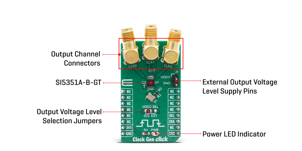
All output drivers generate CMOS level outputs with a single output voltage supply pin (VDDO) allowing a different voltage signal level (1.8, 2.5, or 3.3 V) at the output banks. The output voltage level selection can be chosen by moving an SMD jumper labelled as VDDO SEL to an appropriate position (3V3 or EXT). If 3V3 is chosen, the VDDO is supplied by the board, otherwise, an external supply must be connected to the voltage level supply pin.
The Clock Gen Click Board™ uses the I2C communication interface. It is designed to be operated only with 3.3V logic levels. A proper logic voltage level conversion should be performed before the Click board™ is used with MCUs with logic levels of 5V.
| Type | Clock generator |
| Applications | Audio/video equipment, gaming, printers, scanners, projectors, handheld instrumentation, laser range finder, residential gateways, network/communication, servers, storage, XO replacement. |
| On-board modules | The Clock Gen Click Board™ uses the SI5351A-B-GT IC, a configurable clock generator, from Silicon Labs. |
| Key Features | Configurable clock generator with three outputs, freq generator from 2.5 kHz to 200 MHz, very low power consumption |
| Interface | I2C |
| Compatibility | mikroBUS |
| Click board size | M (42.9 x 25.4 mm) |
| Input Voltage | 3.3V |
This table shows how the pinout of the Clock Gen Click Board™ corresponds to the pinout on the mikroBUS™ socket (the latter shown in the two middle columns).
| Notes | Pin | Pin | Notes | ||||
|---|---|---|---|---|---|---|---|
| NC | 1 | AN | PWM | 16 | NC | ||
| NC | 2 | RST | INT | 15 | NC | ||
| NC | 3 | CS | RX | 14 | NC | ||
| NC | 4 | SCK | TX | 13 | NC | ||
| NC | 5 | MISO | SCL | 12 | SCL | I2C Clock | |
| NC | 6 | MOSI | SDA | 11 | SDA | I2C Data | |
| Power Supply | 3.3V | 7 | 3.3V | 5V | 10 | NC | |
| Ground | GND | 8 | GND | GND | 9 | GND | Ground |
| Label | Name | Default | Description |
|---|---|---|---|
| LD1 | PWR | - | Power LED Indicator |
| JP1 | VDDO SEL | Left | Output voltage level selection 3V3/EXT, left position 3v3, right position External supply |
| Description | Min | Typ | Max | Unit |
|---|---|---|---|---|
| Core Supply Voltage | 3.0 | 3.3 | 3.6 | V |
| Output Buffer Voltage | 1.71 | 3.3 | 3.6 | V |
| Operating Temperature Range | -40 | 25 | 85 | °C |
| Output Impedance | - | 50 | - | Ω |
We provide a library for the Clock Gen Click Board™ on our LibStock page, as well as a demo application (example), developed using MikroElektronika compilers. The demo can run on all the main MikroElektronika development boards.
Library provides functions for communicating with device via I2C module, and many functions for user to easily set frequency of device.
void clockgen_generic_write ( uint8_t reg_adr, uint8_t write_data ) - Function for I2C write to deviceuint8_t clockgen_generic_read ( uint8_t reg_adr ) - Function for I2C read from devicevoid clockgen_set_frequency ( uint8_t clk_num, uint8_t pll_num, uint32_t freq ) - Function for setting frequency to devicevoid clockgen_set_params ( uint8_t clk_pll_num, clockgen_params_t *param_group ) - Function for setting parameters to specific clock or pllvoid clockgen_setup_multisyinth ( uint8_t clk_num, uint32_t divider, uint32_t num, uint32_t denom, uint8_t factor ) - Function for setting OMDvoid clockgen_setup_pll ( uint8_t pll, uint8_t mult, uint32_t num, uint32_t denom ) - Function for setting FMDThe application is composed of three sections :
void application_task ( )
{
 clockgen_set_frequency( CLOCKGEN_CLOCK_0, CLOCKGEN_PLLA, 1 );
 Delay_ms( 5000 );
 clockgen_set_frequency( CLOCKGEN_CLOCK_0, CLOCKGEN_PLLA, 3 );
 Delay_ms( 5000 );
 clockgen_set_frequency( CLOCKGEN_CLOCK_0, CLOCKGEN_PLLA, 10 );
 Delay_ms( 5000 );
 clockgen_set_frequency( CLOCKGEN_CLOCK_0, CLOCKGEN_PLLA, 5 );
 Delay_ms( 5000 );
}
The full application code, and ready to use projects can be found on our LibStock page.
Other mikroE Libraries used in the example:
Depending on the development board you are using, you may need USB UART Click Board™, USB UART 2 Click Board™ or RS232 Click Board™ to connect to your PC, for development systems with no UART to USB interface available on the board. The terminal available in all MikroElektronika compilers, or any other terminal application of your choice, can be used to read the message.
The Clock Gen Click Board™ is supported with mikroSDK - MikroElektronika Software Development Kit. To ensure proper operation of mikroSDK compliant Click board™ demo applications, mikroSDK should be downloaded from the LibStock and installed for the compiler you are using.
- attachments: [{"download_file":[{"download_file":"Clock Gen Click Board™ Schematic"}],"download_filetype":[{"download_filetype":"pdf"}]},{"download_file":[{"download_file":"Silicon Labs Si5351A Clock Generator I2C Interface Datasheet"}],"download_filetype":[{"download_filetype":"pdf"}]}] - device_vendor: Silicon Labs - device_type: SI5351A-B-GT - warranty: 12 months - brand: MikroE - manufacturer: Mikroelektronika d.o.o. - target_keyword: Clock Gen Click Board - brands: gid://shopify/Metaobject/56256004319 - breadcrumbs: ["gid://shopify/Collection/241680580797","gid://shopify/Collection/241553998013","gid://shopify/Collection/279407231165"] - customhs_code: 847330 - detailed_description: {"type":"root","children":[{"type":"heading","level":3,"children":[{"type":"text","value":"How Does The Clock Gen Click Board™ Work?"}]},{"type":"paragraph","children":[{"type":"text","value":"The "},{"type":"text","value":"Clock Gen Click Board™","bold":true,"italic":true},{"type":"text","value":" features the Si5351A, a versatile I2C programmable clock generator that is ideally suited for replacing crystals, crystal oscillators, VCXOs, PLLs, and buffers. The Si5351A consists of an input stage, two synthesis stages, and an output stage. The input stage accepts an external crystal (XTAL on XA and XB pins). The first stage of synthesis multiplies the input frequencies to an high-frequency intermediate clock, while the second stage of synthesis uses high resolution MultiSynth fractional dividers to generate the desired output frequencies. Additional integer division is provided at the output stage for generating output frequencies as low as 2.5 kHz. Crosspoint switches at each of the synthesis stages allows total flexibility in routing any of the inputs to any of the outputs. Because of this high resolution and flexible synthesis architecture, the Si5351A is capable of generating synchronous or free-running non-integer related clock frequencies at each of its outputs, enabling one device to synthesize clocks for multiple clock domains in a design."}]},{"type":"paragraph","children":[{"type":"text","value":""}]},{"type":"paragraph","children":[{"type":"text","value":"The Si5351A uses a fixed-frequency standard AT-cut crystal as a reference to the internal oscillator. The output of the oscillator can be used to provide a free-running reference to one or both of the PLLs for generating asynchronous clocks. The output frequency of the oscillator operates at the crystal frequency of 25 MHz. Internal load capacitors are provided to eliminate the need for external components when connecting a crystal to the Si5351A. The total internal XTAL load capacitance (CL) can be selected to be 0, 6, 8, or 10 pF."}]},{"type":"paragraph","children":[{"type":"text","value":"The Si5351A uses two stages of synthesis to generate its final output clocks. The first stage uses PLLs to multiply the lower frequency input references to a high-frequency intermediate clock. The second stage uses high resolution MultiSynth fractional dividers to generate the required output frequencies. Only two unique frequencies above 112.5 MHz can be simultaneously output. For example, 125 MHz (CLK0), 130 MHz (CLK1), and 150 MHz (CLK2) is not allowed. Both PLLs are locked to the same source (XTAL). The crosspoint switch at the input of the second stage allows any of the MultiSynth dividers to connect to PLLA or PLLB. This flexible synthesis architecture allows any of the outputs to generate synchronous or non-synchronous clocks, with spread spectrum or without spread spectrum, and with the flexibility of generating non-integer related clock frequencies at each output. Frequencies down to 2.5 kHz can be generated by applying the R divider at the output of the Multisynth."}]},{"type":"paragraph","children":[{"type":"text","value":"All output drivers generate CMOS level outputs with a single output voltage supply pin (VDDO) allowing a different voltage signal level (1.8, 2.5, or 3.3 V) at the output banks. The output voltage level selection can be chosen by moving an SMD jumper labelled as VDDO SEL to an appropriate position (3V3 or EXT). If 3V3 is chosen, the VDDO is supplied by the board, otherwise, an external supply must be connected to the voltage level supply pin."}]},{"type":"paragraph","children":[{"type":"text","value":"The "},{"type":"text","value":"Clock Gen Click Board™","bold":true},{"type":"text","value":" uses the I2C communication interface. It is designed to be operated only with 3.3V logic levels. A proper logic voltage level conversion should be performed before the Click board™ is used with MCUs with logic levels of 5V."}]},{"type":"heading","level":3,"children":[{"type":"text","value":"SPECIFICATIONS"}]},{"type":"paragraph","children":[{"type":"text","value":"Type\nClock generator\nApplications\nAudio/video equipment, gaming, printers, scanners, projectors, handheld instrumentation, laser range finder, residential gateways, network/communication, servers, storage, XO replacement.\nOn-board modules\nThe Clock Gen Click Board™ uses the SI5351A-B-GT IC, a configurable clock generator, from Silicon Labs.\nKey Features\nConfigurable clock generator with three outputs, freq generator from 2.5 kHz to 200 MHz, very low power consumption\nInterface\nI2C\nCompatibility\nmikroBUS\nClick board size\nM (42.9 x 25.4 mm)\nInput Voltage\n3.3V"}]},{"type":"heading","level":3,"children":[{"type":"text","value":"PINOUT DIAGRAM"}]},{"type":"paragraph","children":[{"type":"text","value":"This table shows how the pinout of the "},{"type":"text","value":"Clock Gen Click Board™","bold":true},{"type":"text","value":" corresponds to the pinout on the mikroBUS™ socket (the latter shown in the two middle columns)."}]},{"type":"paragraph","children":[{"type":"text","value":"Notes\nPin\nPin\nNotes\nNC\n1\nAN\nPWM\n16\nNC\nNC\n2\nRST\nINT\n15\nNC\nNC\n3\nCS\nRX\n14\nNC\nNC\n4\nSCK\nTX\n13\nNC\nNC\n5\nMISO\nSCL\n12\nSCL\nI2C Clock\nNC\n6\nMOSI\nSDA\n11\nSDA\nI2C Data\nPower Supply\n3.3V\n7\n3.3V\n5V\n10\nNC\nGround\nGND\n8\nGND\nGND\n9\nGND\nGround"}]},{"type":"heading","level":3,"children":[{"type":"text","value":"ONBOARD SETTINGS AND INDICATORS"}]},{"type":"paragraph","children":[{"type":"text","value":"Label\nName\nDefault\nDescription\nLD1\nPWR\n-\nPower LED Indicator\nJP1\nVDDO SEL\nLeft\nOutput voltage level selection 3V3/EXT, left position 3v3, right position External supply"}]},{"type":"heading","level":3,"children":[{"type":"text","value":"CLOCK GEN CLICK ELECTRICAL SPECIFICATIONS"}]},{"type":"paragraph","children":[{"type":"text","value":"Description\nMin\nTyp\nMax\nUnit\nCore Supply Voltage\n3.0\n3.3\n3.6\nV\nOutput Buffer Voltage\n1.71\n3.3\n3.6\nV\nOperating Temperature Range\n-40\n25\n85\n°C\nOutput Impedance\n-\n50\n-\nΩ"}]},{"type":"heading","level":3,"children":[{"type":"text","value":" "}]}]} - summary:The Clock Gen Click Board™ offers an ideal replacement for crystals, crystal oscillators, VCXOs, phase-locked loops (PLLs), and fanout buffers in cost-sensitive applications. This Click Board™ features the Si5351A from Silicon Labs, an I2C configurable clock generator based on a PLL + high-resolution MultiSynth fractional divider architecture which can generate any frequency up to 200 MHz on each of its outputs with 0 ppm error.
The Si5351A is capable of generating synchronous or free-running non-integer related clock frequencies at each of its outputs (CLK0, CLK1, and CLK2), enabling one device to synthesize clocks for multiple clock domains in a design. It eliminates the need for higher cost, custom pullable crystals while providing reliable operation over a wide tuning range. The Si5351C offers the same flexibility but synchronizes to an external reference clock.