When it comes to the TPS55332-Q1, the monolithic high-voltage switching regulator from Texas Instruments, it is important to state that it operates as a step up (boost) converter.
The feedback concept is voltage mode control using the VSENSE terminal, with cycle-by-cycle current limit. The voltage supervisory function for power-on-rest during system power-on is monitoring the output voltage, and once this has exceeded the threshold set by RST_TH, a delay of 1.0 ms/nF (based on the capacitor value on the Cdly terminal) is invoked before the RST line is released high.
The output is sensed through an external resistor divider and compared with an internal reference voltage. The value of the adjustable output voltage in boost mode is selectable between VIN × 1.05 to 50 V if the minimum ON time (ton) and minimum OFF times are NOT violated by choosing the external resistors. The internal reference voltage Vref has a ±1.5% tolerance. The potentiometer featured on the Boost 6 click can change the feedback thus influencing a change in the output voltage. This makes the click extremely practical because you can, with a simple turn of the potentiometer, get the full voltage range.
Once the internal circuits have stabilized with a minimum input supply of 3.6V, the system can then have an input voltage range from 1.5V to 40V, to maintain a fixed boost output voltage.
Over-current protection is implemented by sensing the current through the NMOS switch FET. The sensed current is then compared to a current reference level representing the over-current threshold limit. If the sensed current exceeds the over-current threshold limit, the over-current indicator is set true. The system ignores the over-current indicator for the leading edge blanking time at the beginning of each cycle to avoid any turn-on noise glitches.
The oscillator frequency is selectable by means of a resistor placed at the RT pin. The switching frequency (ƒsw) can be set in the range of 80 kHz to 2.2 MHz.
The power-on reset output is asserted low until the output voltage exceeds the programmed Vreg_RST voltage threshold and the reset delay timer has expired. Additionally, whenever the Enable pin is low or open, RST is immediately asserted low regardless of the output voltage. There is a reset deglitch timer to prevent a reset being invoked due to short negative transients on the output line.
The TPS55332-Q1 device is designed to operate from an input voltage up to 40 V. Ensure that the input supply is well regulated and it can protect itself from overheating with an internal thermal shutdown circuit. If the junction temperature exceeds the thermal shutdown trip point, the MOSFET is turned off. The device is restarted under control of the slow start circuit automatically when the junction temperature drops below the thermal shutdown hysteresis trip point.
Because the Boost 6 Click Board™ is based on the TPS55332-Q1 device, it is deemed ideal for lighting applications, battery powered and automotive applications.
| Type | Boost |
| Applications | Lighting, battery powered applications, automotive applications |
| On-board modules | TPS55332-Q1, a monolithic high-voltage switching regulator from Texas Instruments |
| Key Features | Withstands Transients up to 60 V, Boost Input Operating Range of 1.5 V to 40 V (VIN) |
| Interface | GPIO |
| Compatibility | mikroBUS |
| Click board size | L (57.15 x 25.4 mm) |
| Input Voltage | 3.3V or 5V |
This table shows how the pinout on the Boost 6 Click Board™ corresponds to the pinout on the mikroBUS™ socket (the latter shown in the two middle columns).
| Notes | Pin | Pin | Notes | ||||
|---|---|---|---|---|---|---|---|
| Reset | RST | 1 | AN | PWM | 16 | SYC | Sync |
| Enable | EN | 2 | RST | INT | 15 | NC | |
| NC | 3 | CS | RX | 14 | NC | ||
| NC | 4 | SCK | TX | 13 | NC | ||
| NC | 5 | MISO | SCL | 12 | NC | ||
| NC | 6 | MOSI | SDA | 11 | NC | ||
| Power Supply | 3.3V | 7 | 3.3V | 5V | 10 | 5V | Power Supply |
| Ground | GND | 8 | GND | GND | 9 | GND | Ground |
| Label | Name | Default | Description |
|---|---|---|---|
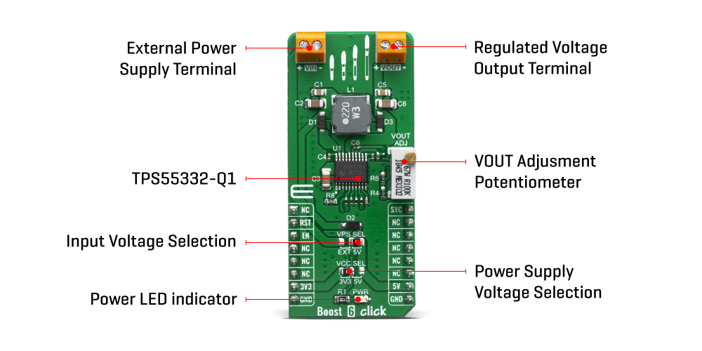
| LD1 | PWR | - | Power LED Indicator |
| JP2 | VCC SEL | Left | Power supply voltage selection: left position 3.3V, right position 5V |
| JP1 | VIN SEL | Right | Input voltage selection: left position – external power supply, right position – 5V from mikroBUS |
| VR1 | VOUT ADJ | - | Output voltage adjusting potentiometer |
Boost 6 Click Board™
- amazon_main_image: https://www.thedebugstore.com/images/product/lg-boost-6-click-3813-front_2.jpg - amazon_other_image_1: https://www.thedebugstore.com/images/product/lg-boost-6-click-3813-back_2.jpg - amazon_other_image_2: https://www.thedebugstore.com/images/product/lg-boost-6-click-3813-fusion_1.jpg - amazon_other_image_3: https://www.thedebugstore.com/images/product/lg-boost-6-click-3813-shuttle_1.jpg - amazon_other_image_4: https://www.thedebugstore.com/images/product/lg-boost-6-click-3813-clicker_1.jpg - amazon_other_image_5: https://www.thedebugstore.com/images/product/lg-boost-6-click-3813-breadboard_1.jpg - amazon_other_image_6: https://www.thedebugstore.com/images/product/lg-boost-6-click-3813-breadboard_1.jpg - amazon_browse_node: 428655031 - mpn: MIKROE-3813 - backorder_label: If no stock shown above, check availability - badge: - widget:We provide a library for the Boost 6 Click Board™ on our LibStock page, as well as a demo application (example), developed using MikroElektronika compilers. The demo can run on all the main MikroElektronika development boards.
The library covers all the necessary functions to control Boost 6 click board.
void boost6_hw_reset( void ) - Hardware reset function.void boost6_power_off( void ) - Power OFF function.void boost6_power_on( void ) - Power ON function.The application is composed of three sections :
void application_task ( )
{
    char receivedData;

    if ( UART_Rdy_Ptr( ) )
    {
        receivedData = UART_Rd_Ptr( );

        switch ( receivedData )
        {
            case 'E' :
            {
                if ( enable_flag == BOOST6_DISABLE )
                {
                    enable_flag = BOOST6_ENABLE;
                    boost6_power_on( );

                    mikrobus_logWrite( "     Enable     ", _LOG_LINE );
                    mikrobus_logWrite( "-----------------", _LOG_LINE );
                }
                break;
            }
            case 'D' :
            {
                if ( enable_flag == BOOST6_ENABLE )
                {
                    enable_flag = BOOST6_DISABLE;
                    boost6_power_off( );

                    mikrobus_logWrite( "     Disable     ", _LOG_LINE );
                    mikrobus_logWrite( "-----------------", _LOG_LINE );
                }
                break;
            }
        }
    }
}

The full application code, and ready to use projects can be found on our LibStock page.
Other mikroE Libraries used in the example:
Depending on the development board you are using, you may need a USB UART click, USB UART 2 click or RS232 click to connect to your PC, for development systems with no UART to USB interface available on the board. The terminal available in all MikroElektronika compilers, or any other terminal application of your choice, can be used to read the message.
The Boost 6 Click Board™ is supported with mikroSDK - MikroElektronika Software Development Kit. To ensure proper operation of mikroSDK compliant Click board™ demo applications, mikroSDK should be downloaded from the LibStock and installed for the compiler you are using.
- attachments: [{"download_file":[{"download_file":"Boost 6 Click Board™ Schematic"}],"download_filetype":[{"download_filetype":"pdf"}]},{"download_file":[{"download_file":"Texas Instruments TPS55332-Q1 Switching Regulator Datasheet"}],"download_filetype":[{"download_filetype":"pdf"}]}] - condition: new - custom_product: false - mpn: MIKROE-3813 - google_product_category: Electronics - custom_label_0: Click Board - device_vendor: Texas Instruments - device_type: TPS55332QPWPRQ1 - warranty: 12 months - brand: MikroE - manufacturer: Mikroelektronika d.o.o. - target_keyword: Boost 6 Click Board - brands: gid://shopify/Metaobject/56256004319 - breadcrumbs: ["gid://shopify/Collection/447955239135","gid://shopify/Collection/241680580797","gid://shopify/Collection/241545478333"] - customhs_code: 847330 - detailed_description: {"type":"root","children":[{"type":"heading","level":3,"children":[{"type":"text","value":"How Does The Boost 6 Click Board™ Work?"}]},{"type":"paragraph","children":[{"type":"text","value":"When it comes to the TPS55332-Q1, the monolithic high-voltage switching regulator from Texas Instruments, it is important to state that it operates as a step up (boost) converter."}]},{"type":"paragraph","children":[{"type":"text","value":"The feedback concept is voltage mode control using the VSENSE terminal, with cycle-by-cycle current limit. The voltage supervisory function for power-on-rest during system power-on is monitoring the output voltage, and once this has exceeded the threshold set by RST_TH, a delay of 1.0 ms/nF (based on the capacitor value on the Cdly terminal) is invoked before the RST line is released high."}]},{"type":"paragraph","children":[{"type":"text","value":""}]},{"type":"paragraph","children":[{"type":"text","value":"The output is sensed through an external resistor divider and compared with an internal reference voltage. The value of the adjustable output voltage in boost mode is selectable between VIN × 1.05 to 50 V if the minimum ON time (ton) and minimum OFF times are NOT violated by choosing the external resistors. The internal reference voltage Vref has a ±1.5% tolerance. The potentiometer featured on the Boost 6 click can change the feedback thus influencing a change in the output voltage. This makes the click extremely practical because you can, with a simple turn of the potentiometer, get the full voltage range."}]},{"type":"paragraph","children":[{"type":"text","value":"Once the internal circuits have stabilized with a minimum input supply of 3.6V, the system can then have an input voltage range from 1.5V to 40V, to maintain a fixed boost output voltage."}]},{"type":"paragraph","children":[{"type":"text","value":"Over-current protection is implemented by sensing the current through the NMOS switch FET. The sensed current is then compared to a current reference level representing the over-current threshold limit. If the sensed current exceeds the over-current threshold limit, the over-current indicator is set true. The system ignores the over-current indicator for the leading edge blanking time at the beginning of each cycle to avoid any turn-on noise glitches."}]},{"type":"paragraph","children":[{"type":"text","value":"The oscillator frequency is selectable by means of a resistor placed at the RT pin. The switching frequency (ƒsw) can be set in the range of 80 kHz to 2.2 MHz."}]},{"type":"paragraph","children":[{"type":"text","value":"The power-on reset output is asserted low until the output voltage exceeds the programmed Vreg_RST voltage threshold and the reset delay timer has expired. Additionally, whenever the Enable pin is low or open, RST is immediately asserted low regardless of the output voltage. There is a reset deglitch timer to prevent a reset being invoked due to short negative transients on the output line."}]},{"type":"paragraph","children":[{"type":"text","value":"The TPS55332-Q1 device is designed to operate from an input voltage up to 40 V. Ensure that the input supply is well regulated and it can protect itself from overheating with an internal thermal shutdown circuit. If the junction temperature exceeds the thermal shutdown trip point, the MOSFET is turned off. The device is restarted under control of the slow start circuit automatically when the junction temperature drops below the thermal shutdown hysteresis trip point."}]},{"type":"paragraph","children":[{"type":"text","value":"Because the "},{"type":"text","value":"Boost 6 Click Board™","bold":true},{"type":"text","value":" is based on the TPS55332-Q1 device, it is deemed ideal for lighting applications, battery powered and automotive applications."}]},{"type":"heading","level":3,"children":[{"type":"text","value":"SPECIFICATIONS"}]},{"type":"paragraph","children":[{"type":"text","value":" "}]},{"type":"paragraph","children":[{"type":"text","value":"Type\nBoost\nApplications\nLighting, battery powered applications, automotive applications\nOn-board modules\nTPS55332-Q1, a monolithic high-voltage switching regulator from Texas Instruments\nKey Features\nWithstands Transients up to 60 V, Boost Input Operating Range of 1.5 V to 40 V (VIN)\nInterface\nGPIO\nCompatibility\nmikroBUS\nClick board size\nL (57.15 x 25.4 mm)\nInput Voltage\n3.3V or 5V"}]},{"type":"paragraph","children":[{"type":"text","value":" "}]},{"type":"heading","level":3,"children":[{"type":"text","value":"PINOUT DIAGRAM"}]},{"type":"paragraph","children":[{"type":"text","value":"This table shows how the pinout on the "},{"type":"text","value":"Boost 6 Click Board™","bold":true},{"type":"text","value":" corresponds to the pinout on the mikroBUS™ socket (the latter shown in the two middle columns)."}]},{"type":"paragraph","children":[{"type":"text","value":"Notes\nPin\nPin\nNotes\nReset\nRST\n1\nAN\nPWM\n16\nSYC\nSync\nEnable\nEN\n2\nRST\nINT\n15\nNC\nNC\n3\nCS\nRX\n14\nNC\nNC\n4\nSCK\nTX\n13\nNC\nNC\n5\nMISO\nSCL\n12\nNC\nNC\n6\nMOSI\nSDA\n11\nNC\nPower Supply\n3.3V\n7\n3.3V\n5V\n10\n5V\nPower Supply\nGround\nGND\n8\nGND\nGND\n9\nGND\nGround"}]},{"type":"heading","level":3,"children":[{"type":"text","value":"ONBOARD SETTINGS AND INDICATORS"}]},{"type":"paragraph","children":[{"type":"text","value":"Label\nName\nDefault\n Description\nLD1\nPWR\n-\nPower LED Indicator\nJP2\nVCC SEL\nLeft\nPower supply voltage selection: left position 3.3V, right position 5V\nJP1\nVIN SEL\nRight\nInput voltage selection: left position – external power supply, right position – 5V from mikroBUS\nVR1\nVOUT ADJ\n-\nOutput voltage adjusting potentiometer"}]},{"type":"heading","level":3,"children":[{"type":"text","value":" "}]}]} - summary:The Boost 6 Click Board™ features the TPS55332-Q1, a monolithic high-voltage switching regulator with integrated 3-A, 60-V power MOSFET. The device can be configured as a switch-mode step-up power supply with a voltage supervisor. This Click Board™ can be used for applications regarding lighting, battery-powered and automotive applications.
The Boost 6 Click is supported by a mikroSDK compliant library, which includes functions that simplify software development. This Click Board™ comes as a fully tested product, ready to be used on a system equipped with the mikroBUS™ socket.